Semiconductor device

a technology of semiconductor devices and semiconductors, applied in the direction of pulse techniques, instruments, computations using denominational number representations, etc., can solve the problems of increasing the cost of chip size while reducing the operation speed, increasing the area penalty, and affecting the security of household electrical appliances, so as to achieve the effect of improving flexibility

Inactive Publication Date: 2011-01-13
RENESAS ELECTRONICS CORP
View PDF10 Cites 3 Cited by
  • Summary
  • Abstract
  • Description
  • Claims
  • Application Information

AI Technical Summary

Benefits of technology

[0016]According to the present embodiment, as the composite module is set in the PM mode or the ePLX mode, the granularity of the circuit configuration is rendered variable, which allows improvement in flexibility when configuring a function.

Problems solved by technology

The conventional programmable device is significantly large in area size as compared to the hardware IP (Intellectual property), which leads to an increase in cost in terms of the chip size while decreasing its operation speed.
However, circuit resources such as a switch element for switching of the wiring between various circuits are incorporated in advance, which causes a problem that the area penalty is significantly increased as compared to the circuit designed in the standard cell such as an ASIC (Application Specific Integrated Circuit).
There is also a problem regarding the security of household electrical appliances.

Method used


Image

  • Semiconductor device
  • Semiconductor device
  • Semiconductor device

Examples


first embodiment

[0043]First, for the purpose of describing the programmable device according to the first embodiment of the present invention, the underlying technique will be described.

[0044]In the following description, the device capable of programming a circuit of about 1-4 bit units will be hereinafter referred to as a fine grain device, and the device capable of programming a circuit of 4 bit units or more will be hereinafter referred to as a coarse grain device.

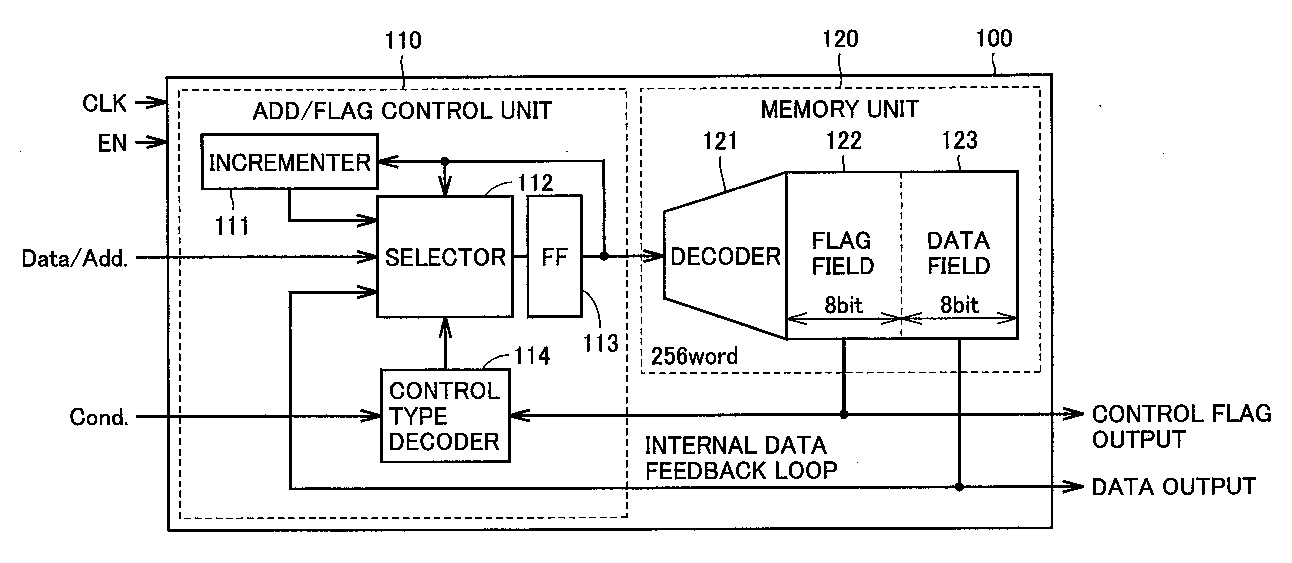
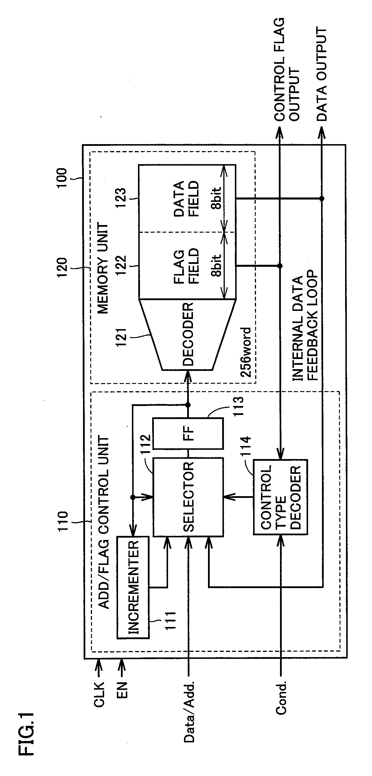
[0045]FIG. 1 is a diagram showing the architecture of a coarse grain device. This coarse grain device 100 can program a state machine, a sequencer, a sequential circuit, and the like, and will be hereinafter referred to as a PA3 (Programmable Autonomous Address-control-memory Architecture). More specifically, see the paper by Yoshifumi

[0046]Kawamura entitled “A Reconfigurable microcomputer system with PA3” (ASSCC2007 Proceeding of Technical paper, pp. 388-391, November, 2007).

[0047]PA3 (100) shown in FIG. 1 includes an Add / Flag contro...

second embodiment

[0101]The second embodiment of the present invention relates to a system equipped with the programmable device described in the first embodiment. Although the system mainly requiring protection of personal information, corporate information and the like, system safety checks, and the like will be hereinafter described, the system is not limited thereto.

[0102]FIG. 20 is a diagram showing a configuration example of the information processing unit equipped with a programmable device in the second embodiment of the present invention. This information processing unit includes a programmable device 1, a CPU 2, a nonvolatile memory 3, an SRAM 4, an I / O and peripheral function IP 5, and a communication Tx / Rx 6. It is to be noted that programmable device 1 has a self- dynamic logic reconfiguration function, and accordingly, will be hereinafter referred to as an SMGP (Scalable Memory Grain Programmable device). Nonvolatile memory 3 also stores the configuration information that is to be set i...


PUM


Abstract

An ePLX unit includes a logic unit having an SRAM and a MUX, and a switch unit having an SRAM and a TG for establishing wiring connection in the logic unit. When a composite module is set in the first mode, an Add / Flag control unit uses the SRAMs as a data field and a flag field, respectively, to autonomously control the read address of each of the data field and the flag field in accordance with a control flag stored in the flag field. Furthermore, when the composite module is set in the second mode, the Add / Flag control unit writes configuration information into each of the SRAMs to reconfigure a logic circuit. Consequently, the granularity of the circuit configuration can be rendered variable, which allows improvement in flexibility when configuring a function.

Description

TECHNICAL FIELD[0001]The present invention relates to a semiconductor device capable of programming a configuration of a logic circuit, and more particularly to a semiconductor device providing a circuit configuration having granularity rendered variable to allow improvement in flexibility in configuring a function.BACKGROUND ART[0002]In recent years, in the field of digital equipment such as digital household electrical appliances, personal computers, mobile phones, automobile applications, and white goods, there is an increasing need to improve security by remote diagnosis via a network and to improve system security by self-diagnosis. The above-described needs have been taken into consideration because of the necessity of system monitoring, protection of personal information and the like in terms of security. Furthermore, these techniques will be incorporated in devices as an encryption function and an authentication function for personal / system devices in the field of digital co...

Claims


Application Information

Patent Timeline
Patent Type & Authority Applications(United States)
IPC IPC(8): H03K19/173
CPCH03K19/17756H03K19/1733
Inventor ARIMOTO, KAZUTAMI
Owner RENESAS ELECTRONICS CORP
Why Eureka
Try Eureka