
Film forming method and substrate processing apparatus

a technology of substrate processing and forming method, which is applied in the direction of coating, coating, chemical vapor deposition coating, etc., can solve the problems of increasing resistance and difficult to form good tisisub>x/sub>film, and achieve the reduction of the effect of reducing the thermal budget of a semiconductor device and preventing the degradation of electrical characteristics attributable to high-temperature processing

Active Publication Date: 2010-12-02
TOKYO ELECTRON LTD
View PDF5 Cites 11 Cited by
  • Summary
  • Abstract
  • Description
  • Claims
  • Application Information

AI Technical Summary

Benefits of technology

The present invention provides a method for efficiently forming a high-quality titanium film or titanium silicide film on a target substrate at low temperature. The method includes a titanium silicide film formation step and a titanium film formation step. The titanium silicide film formation step involves introducing titanium compound gas into the processing chamber, removing the gas through a purging process, and reacting the gas with silicon on the substrate surface to form a titanium silicide film. The titanium film formation step involves generating plasma in the chamber, introducing titanium compound gas and hydrogen gas, and reacting the gas with silicon on the substrate surface to form a titanium film. The method also includes a substrate processing apparatus for controlling the temperature and pressure in the processing chamber. The invention can effectively reduce impurities in the titanium silicide film and titanium film, and can form a barrier layer including both titanium silicide and titanium films in a short period of time. The method can also reduce the thermal budget and prevent degradation of electrical characteristics in semiconductor devices.

Problems solved by technology

However, when a Ti film is formed at low temperature using conventional plasma CVD, there is a problem in that a large amount of Cl remains in the Ti film, thus increasing the resistance of the Ti film.
However, since a Ti film formed by executing plasma SFD at a low temperature of, for example, 450° C. or less cannot be easily silicided, it is difficult to form a good TiSix film.

Method used


Image

  • Film forming method and substrate processing apparatus
  • Film forming method and substrate processing apparatus
  • Film forming method and substrate processing apparatus

Examples


Embodiment Construction

[0125]Hereinafter, embodiments of the present invention will be described in detail with reference to the attached drawings. The same reference numerals are used throughout the different drawings to designate the same or similar components, and thus a repeated description thereof is omitted.

[0126](Example of Construction of Substrate Processing Apparatus)

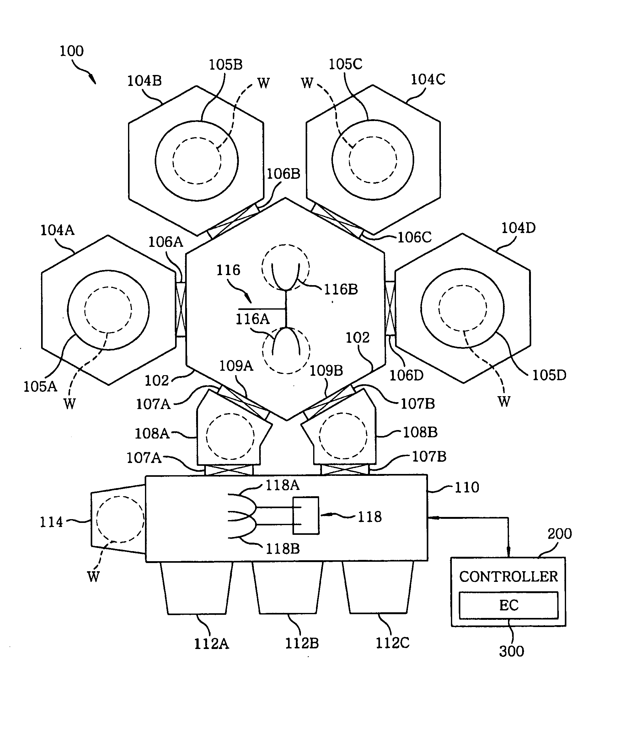
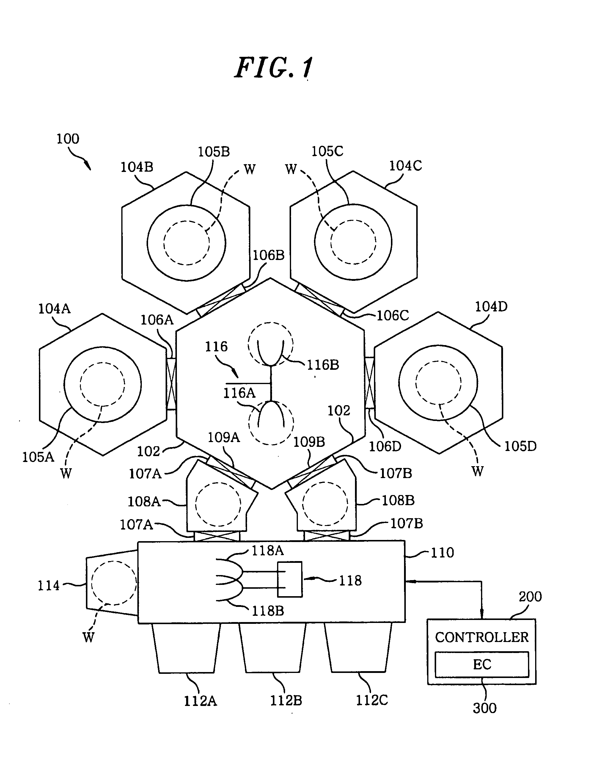
[0127]An example of the construction of a substrate processing apparatus according to an embodiment of the present invention is described below with reference to the drawings. FIG. 1 is a diagram schematically showing an example of the substrate processing apparatus according to the present embodiment. As shown in FIG. 1, the substrate processing apparatus 100 includes a common transfer chamber 102 formed in an approximately polygonal shape (for example, a hexagonal shape), a plurality of (for example, 4) processing chambers 104A to 104D configured to form a vacuum, two load-lock chambers 108A and 108B configured to form a vacuum, a...


PUM

PropertyMeasurementUnit
temperatureaaaaaaaaaa
timeaaaaaaaaaa

Abstract

A barrier layer including a titanium film is formed at a low temperature, and a TiSix film is self-conformably formed at the interface between the titanium film and the base. In forming the TiSix film 507, the following steps are repeated without introducing argon gas: a first step of introducing a titanium compound gas into the processing chamber to adsorb the titanium compound gas onto the silicon surface of a silicon substrate 502; a second step of stopping introduction of the titanium compound gas into the processing chamber and removing the titanium compound gas remaining in the processing chamber; and a third step of generating plasma in the processing chamber while introducing hydrogen gas into the processing chamber to reduce the titanium compound gas adsorbed on the silicon surface and react it with the silicon in the silicon surface to form the TiSix film 507.

Description

FIELD OF THE INVENTION[0001]The present invention relates to a film forming method and substrate processing apparatus for forming a predetermined film on a target substrate such as a semiconductor wafer or a flat panel display (FPD) substrate.BACKGROUND OF THE INVENTION[0002]A semiconductor device, such as a CMOS transistor, has a connection structure including a wiring layer and a substrate, or a wiring layer and another wiring layer. In detail, as shown in FIG. 17, a contact hole 20 is formed between the P / N impurity diffusion layer (diffusion layer) 10 of a Si substrate (Si wafer) and a first wire, and a via hole 30 is formed between the first wire and a second wire. The contact hole 20 and via hole 30 are filled with metal such as tungsten or copper, and are electrically connected to the Si substrate or a wiring layer. Recently, prior to the filling of metal, barrier layers, such as Ti / TiN laminate layers, are formed in the contact hole 20 and the via hole 30, and thus barrier l...

Claims


Application Information

Patent Timeline
Patent Type & Authority Applications(United States)
IPC IPC(8): H01L21/285H05H1/00
CPCC23C16/14C23C16/34C23C16/45512C23C16/4554C23C16/45542H01L21/28518H01L21/28562H01L21/67207H01L21/76814H01L21/76843H01L21/3205
Inventor NARUSHIMA, KENSAKUAMANO, FUMITAKAWAKABAYASHI, SATOSHI
Owner TOKYO ELECTRON LTD
Learn More