Solar Cell and Solar Cell Manufacturing Method
- Summary
- Abstract
- Description
- Claims
- Application Information
AI Technical Summary
Benefits of technology
Problems solved by technology
Method used
Image
Examples
first preferred embodiment
[0021]>
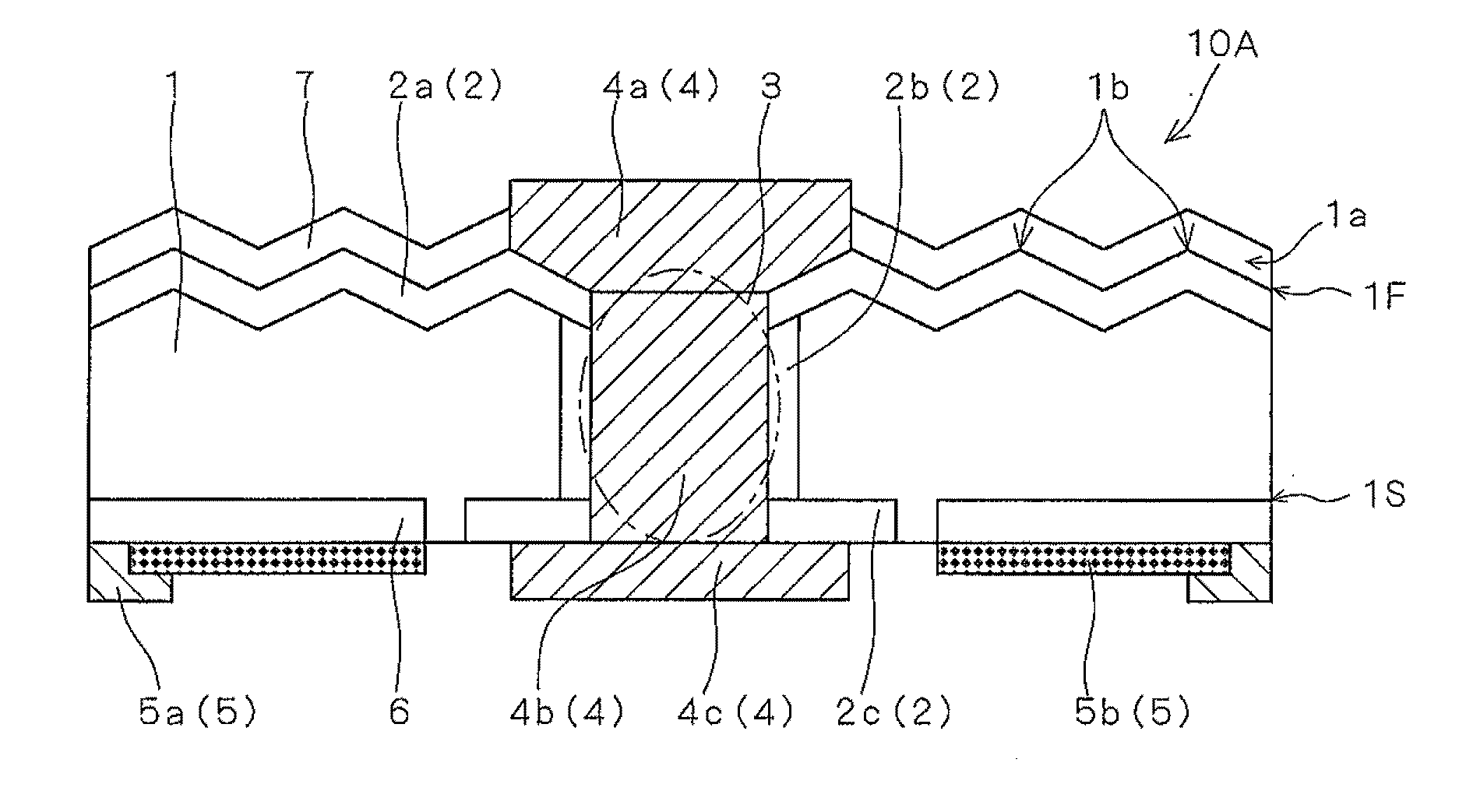
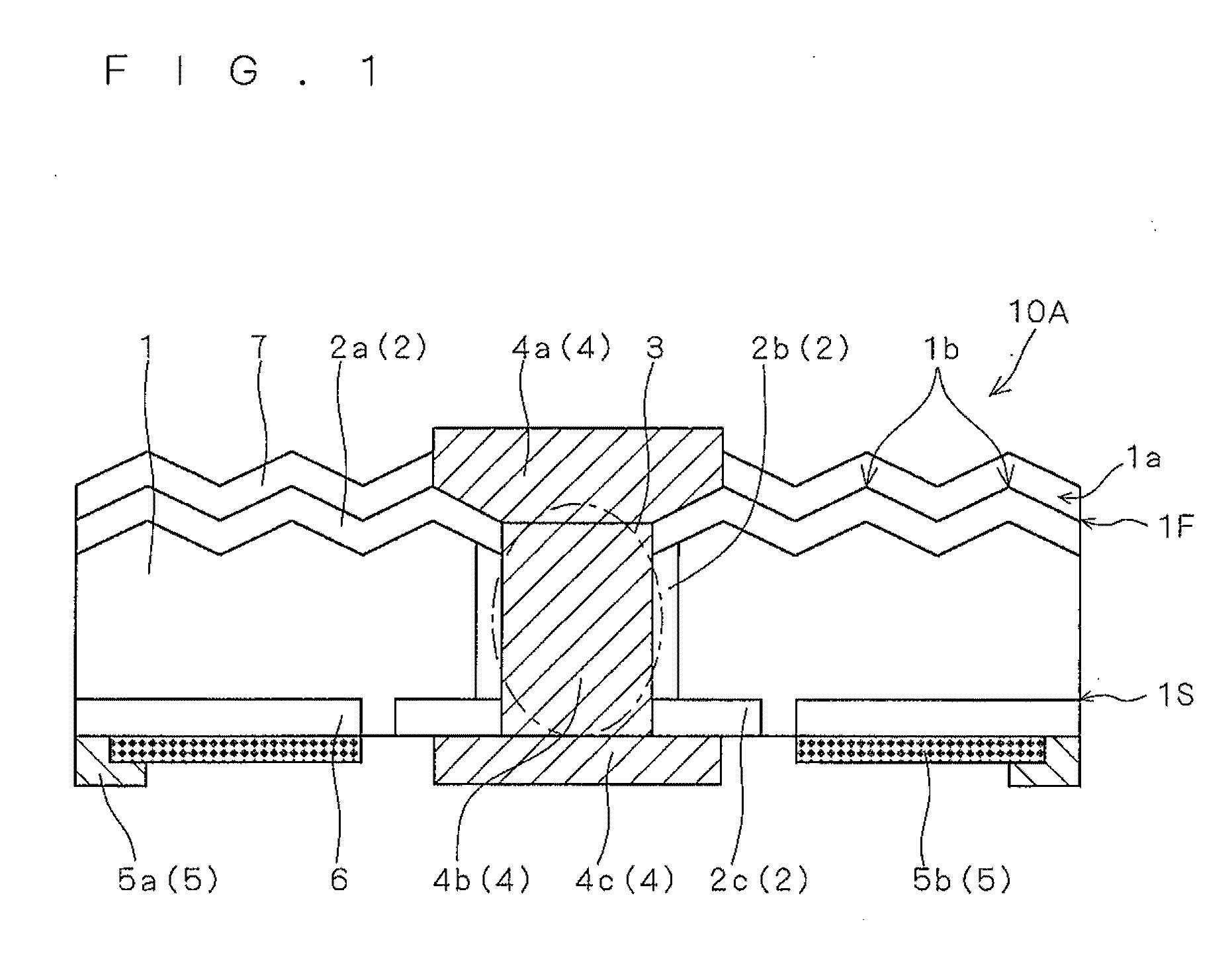
[0022]FIG. 1 is a schematic cross-sectional diagram showing a configuration of a solar cell 10A according to a first preferred embodiment of the present invention.
[0023]The solar cell 10A includes a semiconductor substrate 1 having one conductivity type, an opposite conductivity type layer 2 having a different conductivity type from the semiconductor substrate 1, a first electrode 4, and a second electrode 5.
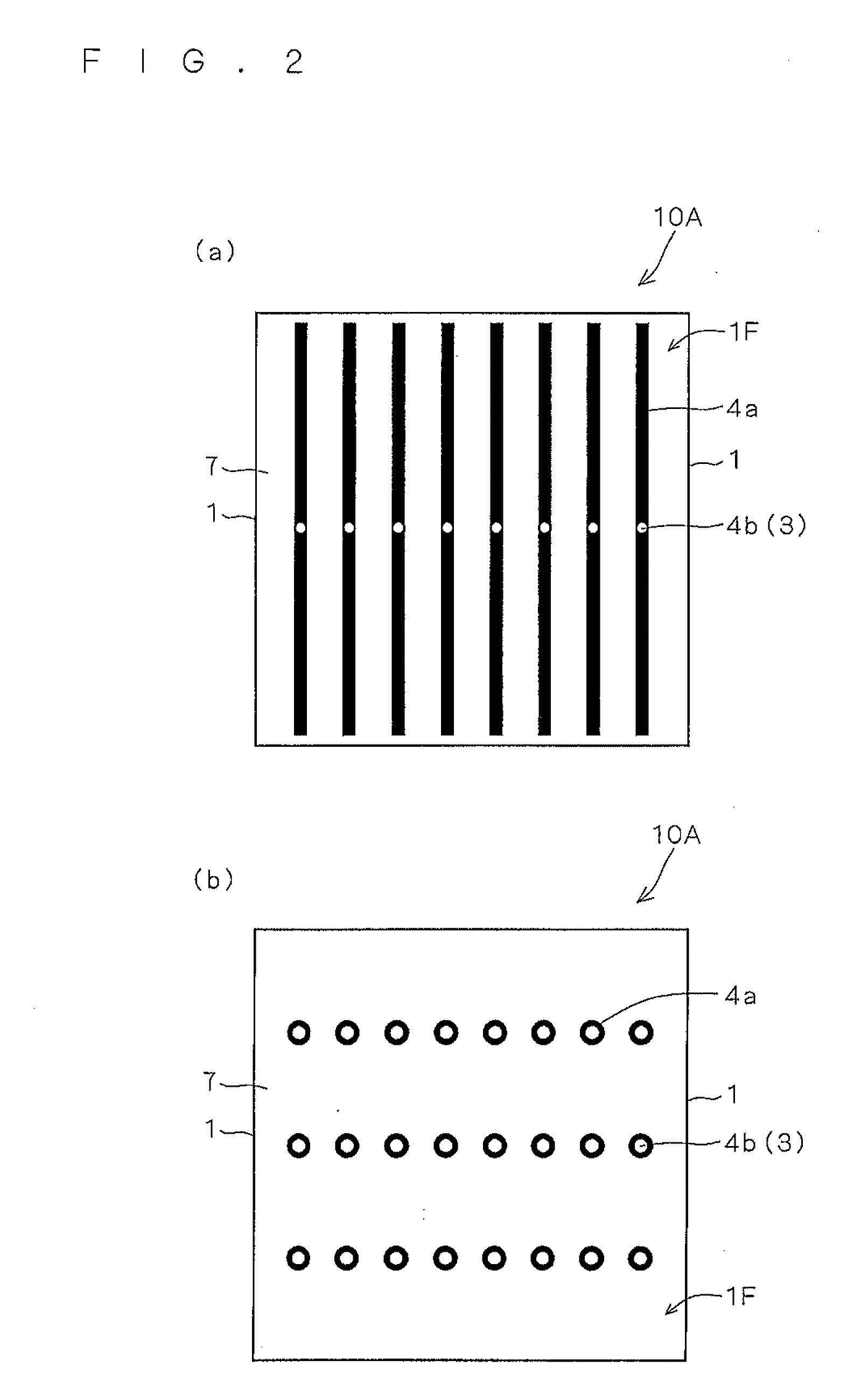
[0024]The solar cell 10A includes the semiconductor substrate 1 that has a first surface 1F (in FIG. 1, the top surface) and a second surface 1S (in FIG. 1, the bottom surface) on the back side of the first surface 1F. In the case of the solar cell 10A, the first surface 1F is the light receiving surface (for convenience of description, the first surface 1F may also be referred to as the light receiving surface of the semiconductor substrate 1, or the like).
[0025]The semiconductor substrate 1 may be a crystalline silicon substrate, such as a single crystalline silicon sub...
second preferred embodiment
[0123]FIG. 6 is a schematic cross-sectional diagram showing a configuration of a solar cell 10B according to a second preferred embodiment of the present invention. The solar cell 10B according to the present preferred embodiment differs from the solar cell 10A according to the first preferred embodiment in the structure of the first electrode 4. Thus, those components that have the same functions and effects as the components of the solar cell 10A are denoted by the same reference numerals and characters, and their description will be omitted herein.
[0124]In the solar cell 10B according to the present preferred embodiment, the main electrode portion 4a consists of two layers, namely a contact portion (second portion) 4d and a non-contact portion (first portion) 4e. The contact portion 4d is a part that is connected directly to the first opposite conductivity type layer 2a. On the other hand, the non-contact portion 4e is a part that is formed on the contact portion 4d as well as co...
third preferred embodiment
[0137]FIG. 8 is a schematic cross-sectional diagram showing a configuration of a solar cell 10C according to a third preferred embodiment of the present invention. The solar cell 10C according to the present preferred embodiment includes components similar to those of the solar cell 10A according to the first preferred embodiment, but differs from the solar cell 10A in that the through holes 3 have roughened surfaces (have an uneven structure).
[0138]With through holes 3 so configured, even in the case where the conducting portion 4b is formed with a conductive paste having a low glass content as described above, the adhesion of the conducting portion 4b to the second opposite conductivity type layer 2b can be improved by an anchoring effect. Both the heights and widths of the projections on the surfaces of the through holes 3 may preferably be 30 μm or less.
[0139]Such surface roughening is performed by, after forming the through holes 3 as shown in FIG. 4(b), etching the semiconduct...
PUM
 Abstract
Description
Claims
Application Information
 - R&D
- Intellectual Property
- Life Sciences
- Materials
- Tech Scout
- Unparalleled Data Quality
- Higher Quality Content
- 60% Fewer Hallucinations
Browse by: Latest US Patents, China's latest patents, Technical Efficacy Thesaurus, Application Domain, Technology Topic, Popular Technical Reports.
© 2025 PatSnap. All rights reserved.Legal|Privacy policy|Modern Slavery Act Transparency Statement|Sitemap|About US| Contact US: help@patsnap.com


