Semiconductor device and method of manufacturing the same
a technology of semiconductors and semiconductors, applied in the direction of semiconductor devices, basic electric elements, electrical equipment, etc., can solve the problems of increasing impact ionization ratio and degradation of electric characteristics, and achieve the effect of inhibiting the degradation of electric characteristics and reducing electric field concentration
- Summary
- Abstract
- Description
- Claims
- Application Information
AI Technical Summary
Benefits of technology
Problems solved by technology
Method used
Image

Examples
embodiment 1
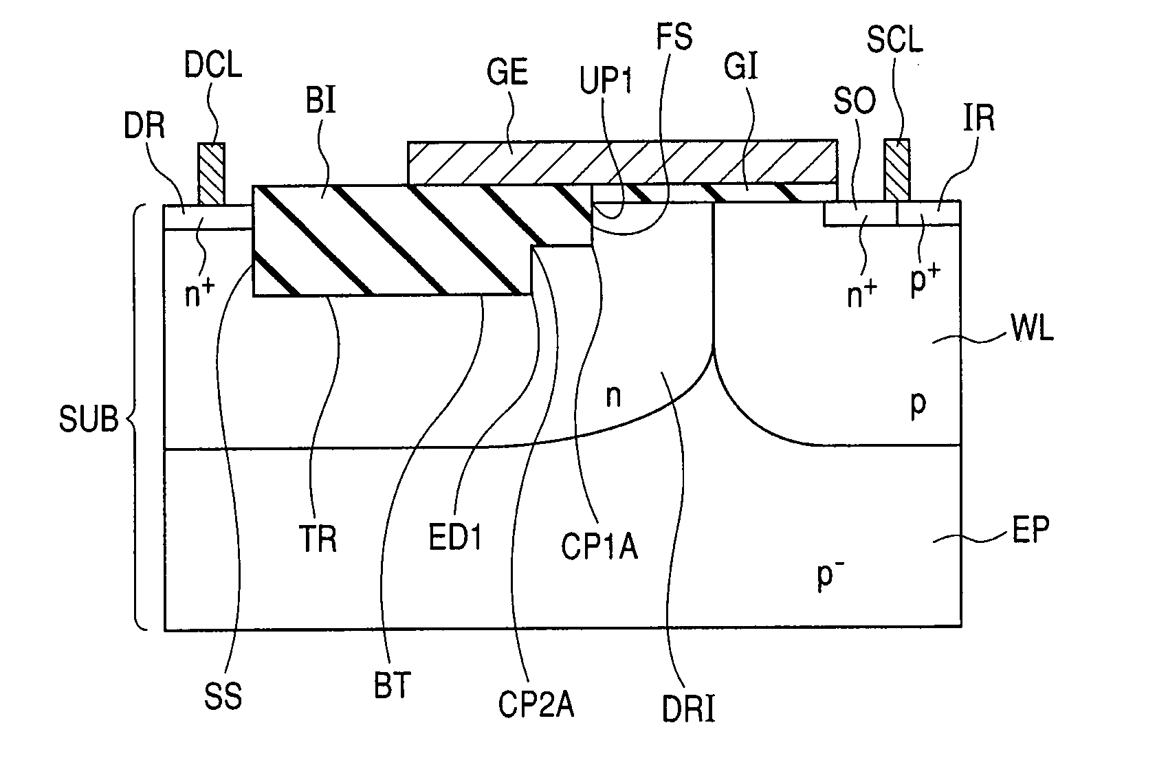
[0073]First, a configuration of a semiconductor device in Embodiment 1 will be described using FIGS. 1 and 2.
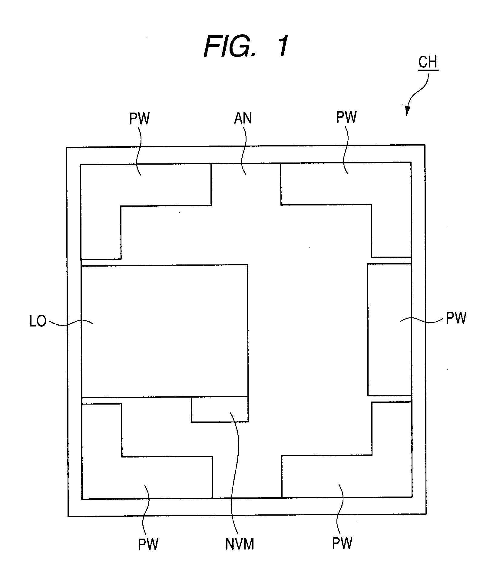
[0074]Referring to FIG. 1, an analog / digital mixed chip CH has, e.g., an analog element formation region AN, a logic element formation region LO, a memory element formation region NVM, and a power element formation region PW. In the analog element formation region AN, formed is an analog device such as, e.g., a resistor. In the logic element formation region LO, formed is, e.g., a complementary MOS (CMOS) transistor or the like. In the memory element formation region NVM, formed is, e.g., a stacked-gate nonvolatile memory or the like. In the power element formation region PW, formed is, e.g., an LDMOS transistor or the like.
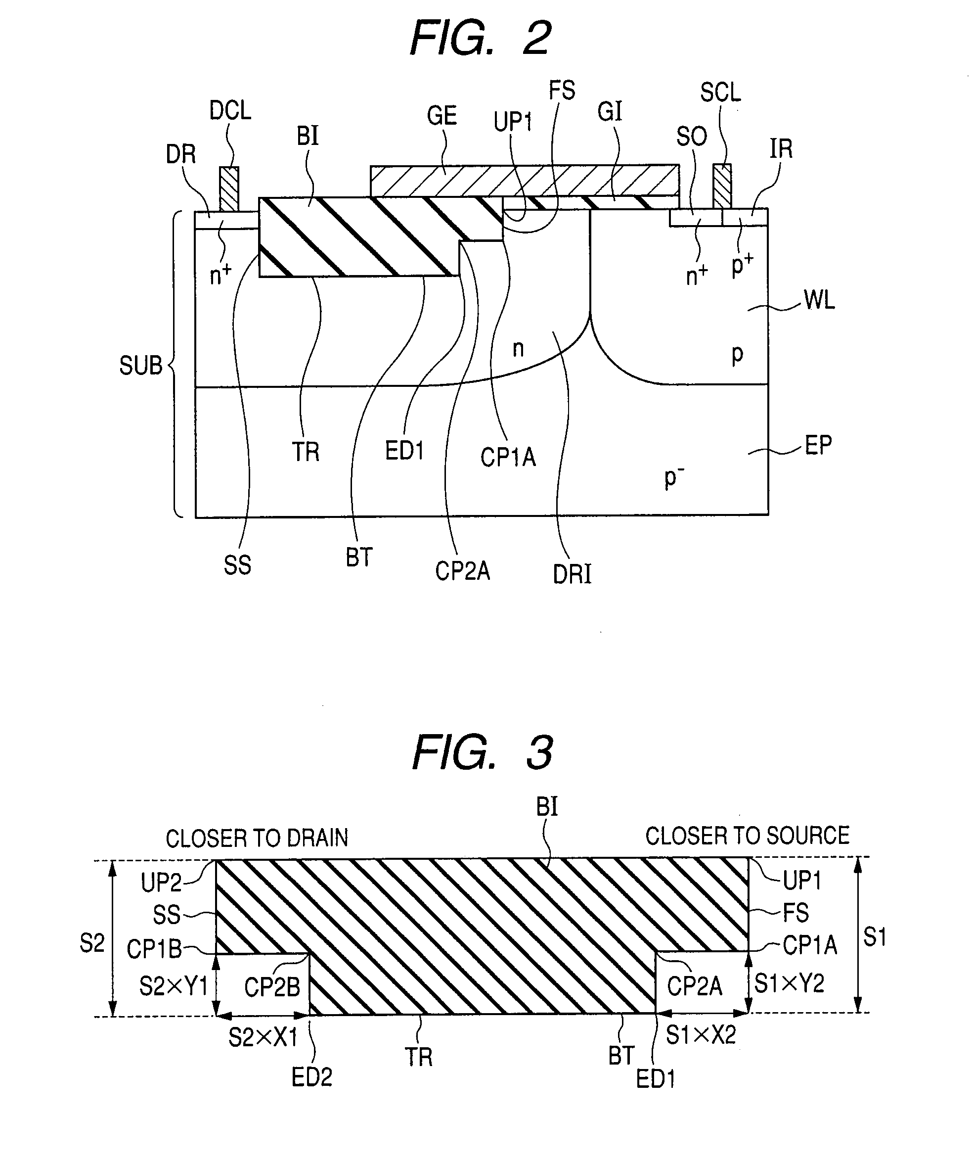
[0075]Referring to FIG. 2, the LDMOS transistor described above primarily has a semiconductor substrate SUB, an n+ source region (first region) SO, an n+ drain region (second region) DR, a p-type well region (third region) WL, an n-type drift region (fourt...
embodiment 2
[0114]Next, a configuration of a semiconductor device according to Embodiment 2 will be described using FIG. 21.
[0115]Referring to FIG. 21, the configuration of the present embodiment is different from the configuration of Embodiment 1 shown in FIG. 2 in that the other wall portion SS of the trench TR closer to the drain has a stepped shape, while the one wall portion FS of the trench TR closer to the source does not have a stepped shape. In the configuration of the present embodiment, the other wall portion SS of the trench TR has a projecting angular portion CP1B and a depressed angular portion CP2B to show a stepped shape when viewed in cross section.
[0116]The two angular portions CP1B and CP2B are located between an upper portion UP2 of the trench TR located in the main surface of the semiconductor substrate SUB and the bottom portion BT thereof. Note that, in the present embodiment, the angular portions located between the upper portion TP2 and the bottom portion BT of the tren...
embodiment 3
[0131]Next, a configuration of a semiconductor device according to Embodiment 3 will be described using FIG. 27.
[0132]Referring to FIG. 27, the configuration of the present embodiment is different from the configuration of Embodiment 1 shown in FIG. 2 in that not only the one wall portion FS of the trench TR closer to the source, but also the other wall portion SS of the trench RT closer to the drain have respective stepped shapes. In the configuration of the present embodiment, the one wall portion FS of the trench TR closer to the source has the projecting angular portion CP1A and the depressed angular portion CP2A to show a stepped shape when viewed in cross section. On the other hand, the other wall portion SS of the trench TR closer to the drain has the projecting angular portion CP1B and the depressed angular portion CP2B to also show a stepped shape when viewed in cross section.
[0133]The two angular portions CP1A and CP2A of the one wall portion FS are located between the upp...
PUM
 Abstract
Description
Claims
Application Information
 - R&D
- Intellectual Property
- Life Sciences
- Materials
- Tech Scout
- Unparalleled Data Quality
- Higher Quality Content
- 60% Fewer Hallucinations
Browse by: Latest US Patents, China's latest patents, Technical Efficacy Thesaurus, Application Domain, Technology Topic, Popular Technical Reports.
© 2025 PatSnap. All rights reserved.Legal|Privacy policy|Modern Slavery Act Transparency Statement|Sitemap|About US| Contact US: help@patsnap.com