Method for depositing ceramic thin film by sputtering using non-conductive target

a ceramic thin film and target technology, applied in the field of ceramic thin film sputtering with a non-conductive target, can solve the problems of poor battery yield, difference in deposition rate, processing speed and precision recall not meeting the commercialization requirement, etc., to improve the uniformity of deposited thin film, reduce the processing time, and low power

Inactive Publication Date: 2010-10-21
APPLIED MATERIALS INC
View PDF10 Cites 14 Cited by
  • Summary
  • Abstract
  • Description
  • Claims
  • Application Information

AI Technical Summary

Benefits of technology

[0022]The hybrid power in combination of the DC power and the AC/RF power in accordance with the present invention can be advantageously used for the manufacture of thin film batteries through sputtering of a lithium metal oxide-based active cathode material, which particularly contributes to decreasing the thin film deposition processing time and to improving uniformity of the deposited thin film.
[0023]With the use of the hybrid power, the AC/RF power can be involved only in the plasma production so a relatively low-price, low-power AC/RF output can be utilized, instead of the conventional high-price, high-power AC/RF output used for the m

Problems solved by technology

Although all-solid-state thin film lithium batteries have many advantages, differences in deposition rates of the respective thin films forming such a battery and a poor yield on the batteries because of the (relatively slow) deposition rat

Method used


Image

  • Method for depositing ceramic thin film by sputtering using non-conductive target
  • Method for depositing ceramic thin film by sputtering using non-conductive target
  • Method for depositing ceramic thin film by sputtering using non-conductive target

Examples


Embodiment Construction

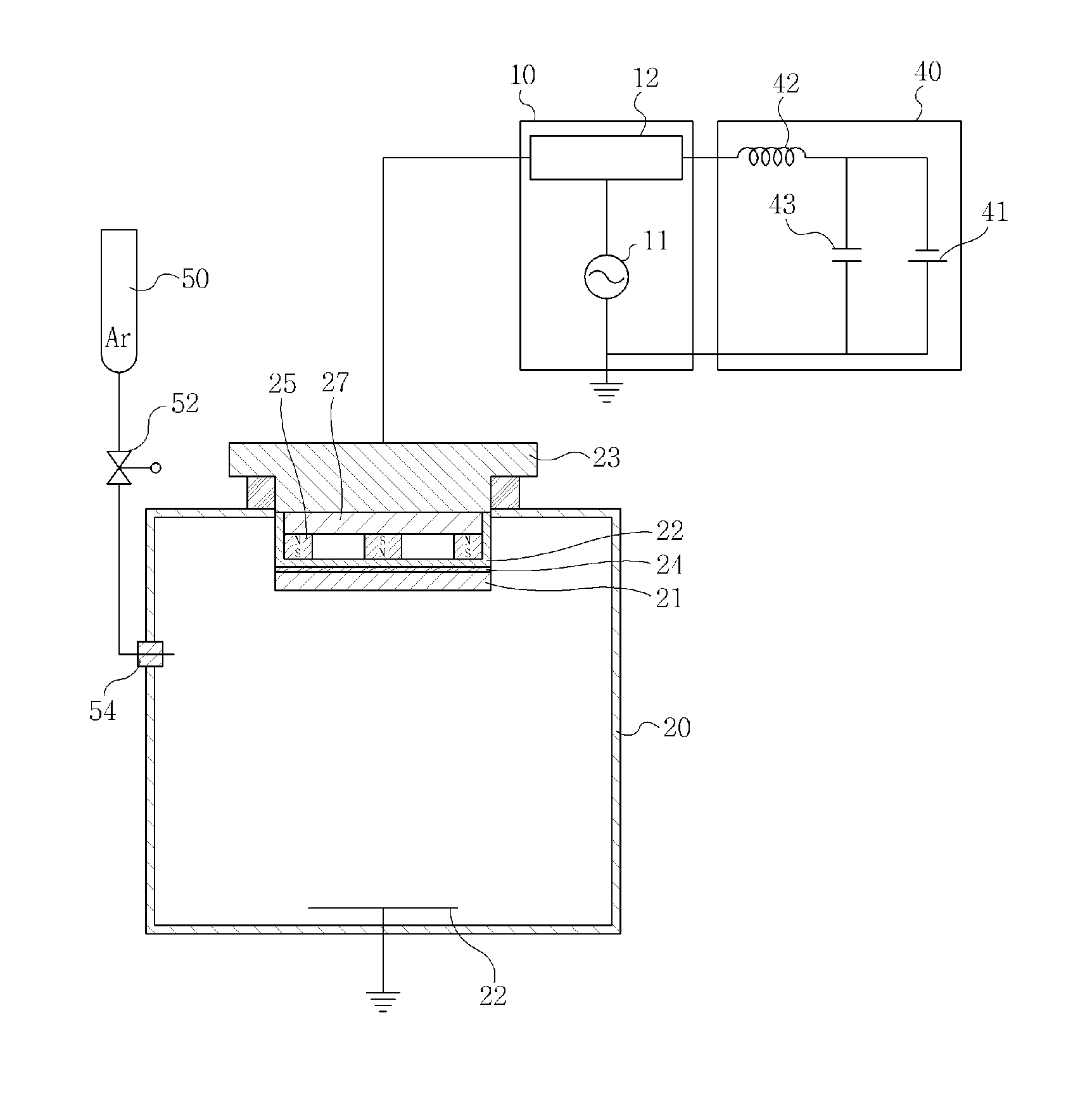
[0033]Hereinafter, preferred embodiments of the present invention will be described in detail with reference to the accompanying drawings.

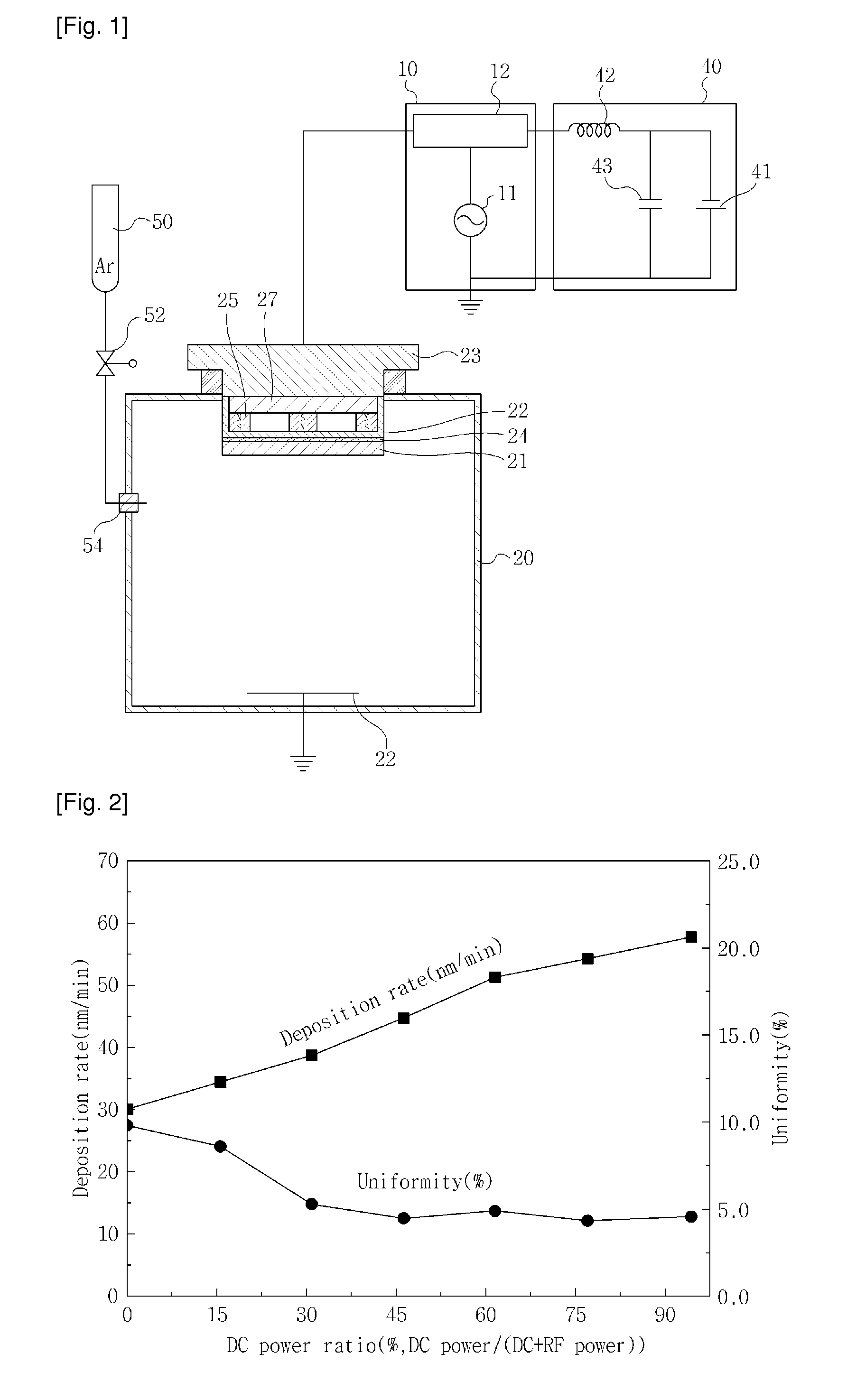
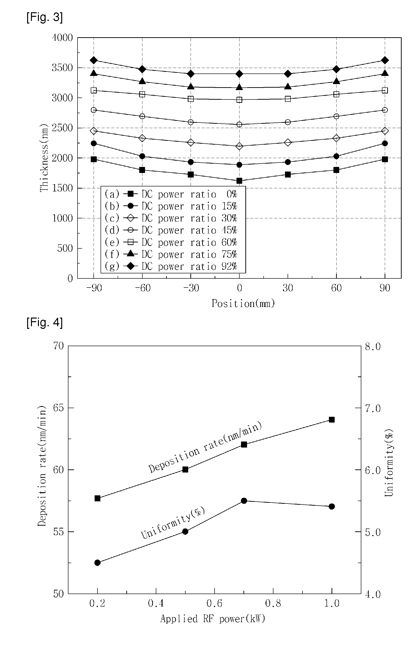
[0034]After the inventors have dedicated much efforts to developing a technique for increasing deposition rate that is regarded as the biggest problem in the conventional RF sputtering process on a nonconductive target, they learned that the sputtering deposition rate of a thin film could be increased when an AC / RF power is first applied to a nonconductive target to form plasma within a chamber and then a hybrid power in combination of an AC / RF power and a DC power is applied to the target, such that the applied DC power from a hybrid power supply is used as power for sputtering the plasma in the chamber after all. Another unexpected fact the inventors have discovered that even the uniformity of the deposited thin film got improved by the new technique, compared to that of the deposited thin film done by the conventional sputtering.

[0035]Under suc...


PUM

PropertyMeasurementUnit
Fractionaaaaaaaaaa
Poweraaaaaaaaaa
Compositionaaaaaaaaaa

Abstract

A method for depositing a ceramic thin film by sputtering is provided to increase deposition rate of the ceramic thin film and to enhance the uniformity of a deposited thin film, which are accomplished by positioning a nonconductive target within a vacuum chamber, and applying an AC/RF power to the target to produce plasma within the chamber, followed by the application of a hybrid power in combination of an AC/RF power and a DC power to the target to proceed a sputtering process inside the vacuum chamber, such that the ceramic thin film is deposited on a substrate placed in the vacuum chamber.

Description

TECHNICAL FIELD[0001]The present invention relates to a method and an apparatus for depositing a ceramic thin film by sputtering using a non-conductive target. Examples of such a ceramic thin film for which the present invention can be implemented include lithium metal oxide thin films such as LiCoO2, LiMn2O4, LiNiO2 and so forth, which are used as a cathode for a secondary thin film lithium battery, and CIGS (Cu(In, Ca)Se2) used as a semiconductor material for a solar cell. In particular, the following description will focus on a method for depositing a LiCoO2 thin film, the most essential element for a all-solid-state secondary thin film lithium battery, by sputtering using a non-conductive LiCoO2 target.BACKGROUND ART[0002]Although all-solid-state thin film lithium batteries have many advantages, differences in deposition rates of the respective thin films forming such a battery and a poor yield on the batteries because of the (relatively slow) deposition rate of ceramic-based fi...

Claims


Application Information

Patent Timeline
IPC IPC(8): C23C14/34
CPCC23C14/0623C23C14/08C23C14/35H01J37/3405Y02E60/122H01L21/02568H01L21/02631H01M4/0426H01M4/1391H01J37/3426Y02E60/10H01L21/203
Inventor NAM, SANG-CHEOLPARK, HO-YOUNGLIM, YOUNG-CHANGLEE, KI-CHANGCHOI, KYU-GILHWANG, HO-SUNGPARK, GI-BACK
Owner APPLIED MATERIALS INC
Why Eureka
Try Eureka