Ring-Based Multi-Push Voltage-Controlled Oscillator
a voltage control and oscillator technology, applied in the field of ring-based multi-push voltage control oscillators, can solve the problems of difficult implementation of multi-push vco design, low practicability of oscillator, and circuit cannot tune output frequency, so as to increase the tuning frequency range and operation frequency, enhance the output power, and reduce the area of the circuit
- Summary
- Abstract
- Description
- Claims
- Application Information
AI Technical Summary
Benefits of technology
Problems solved by technology
Method used
Image
Examples
first embodiment
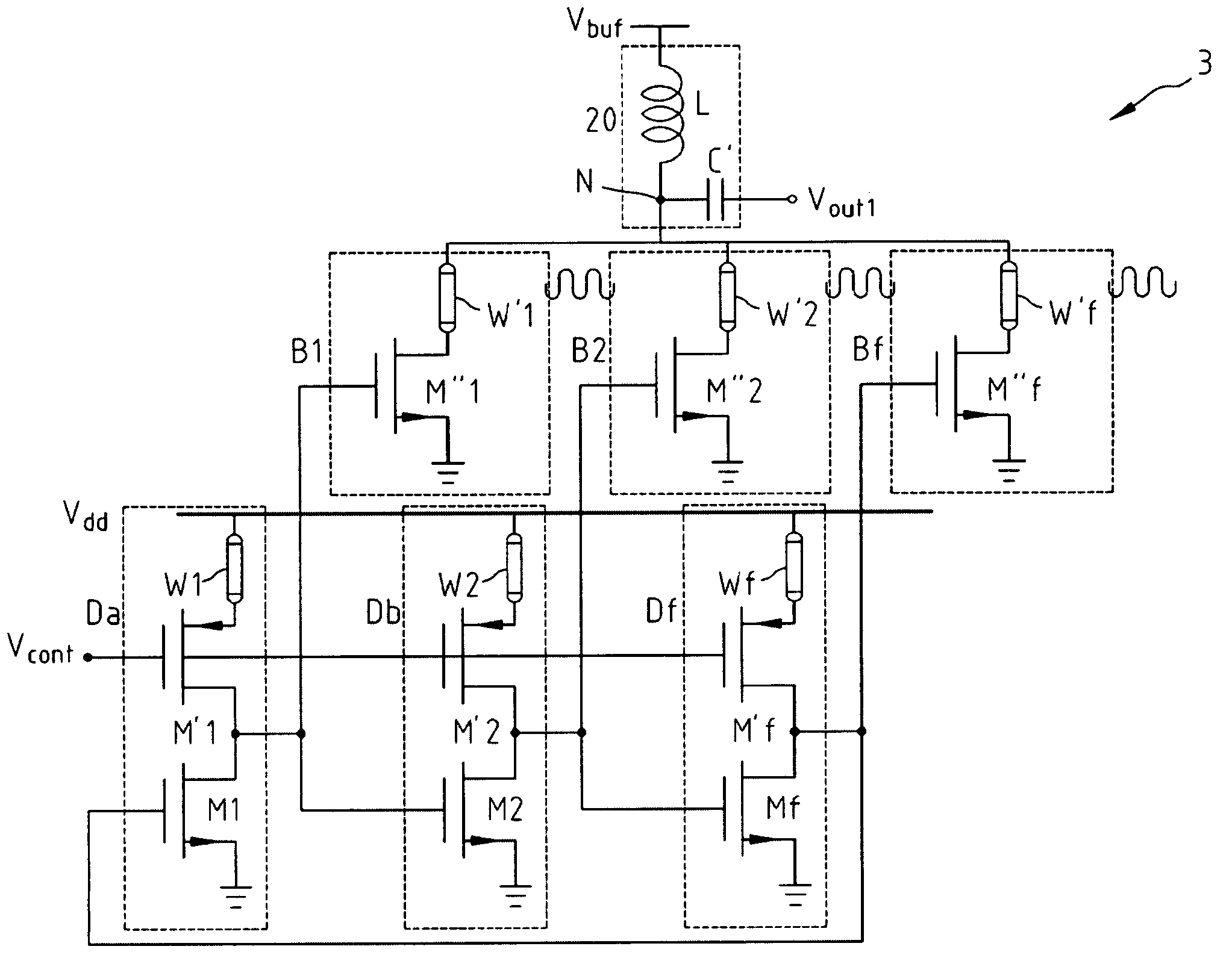
[0021]FIG. 3 is a diagram illustrating the first embodiment according to the present invention with use of three delay cells to implement the ring-based triple-push VCO 3 so as to explain the technological skills of the present invention. However, the present invention can be a ring-based multiple-push VCO that has a plurality of delay cells. The ring-based triple-push VCO 3 comprises a first delay cell D1, a second delay cell D2, a last delay cell Df, a first buffer amplifier B1, a second buffer amplifier B2, a last buffer amplifier Bf, and a bias unit 20. The first delay cell D1, the second delay cell D2, and the last delay cell Df receive a control voltage Vcont for controlling the frequency of the ring-based triple-push VCO 3. When the control voltage Vcont increases, the signal frequency decreases.
[0022]The power source terminals of the first delay cell D1, the second delay cell D2, and the last delay cell Df connect with the power voltage Vdd. The ground terminals of the first...
second embodiment
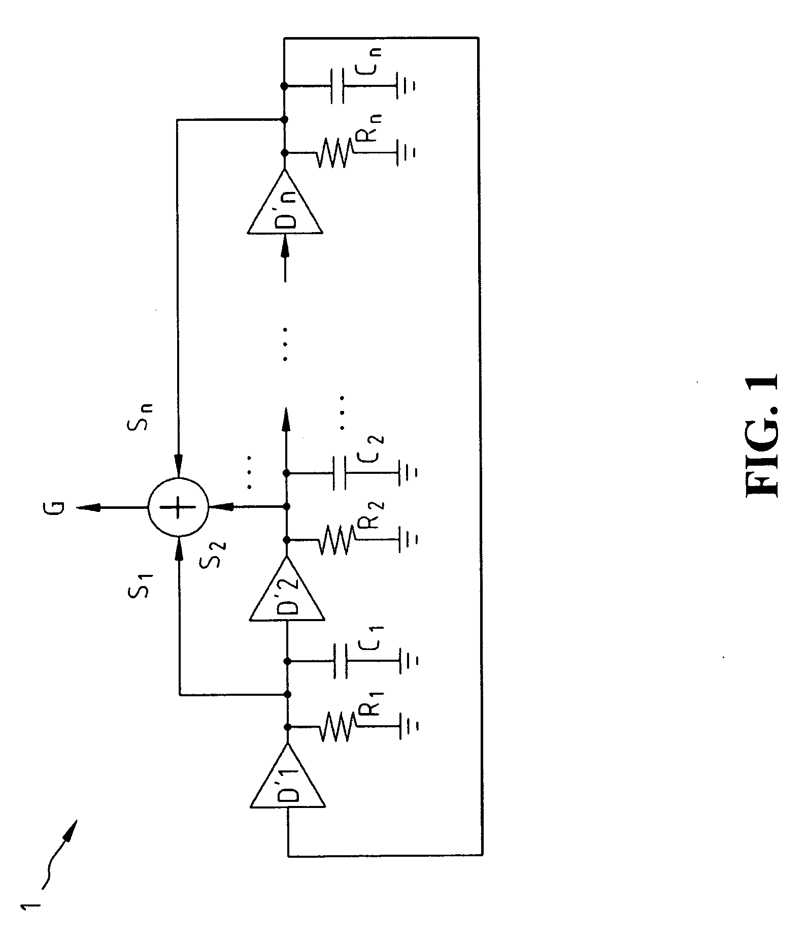
[0029]FIG. 4 is a diagram illustrating the second embodiment according to the present invention, in which n delay cells, n buffer amplifiers, and a bias unit 20 are used, and n is a positive integer that great than 3. The n delay cells comprise a first delay cell D1, a second delay cell D2, . . . , and a nth delay cell Dn. Each delay cell receives the control voltage Vcont. The power source terminal of each delay cell connects with the power voltage Vdd, the ground terminal of each delay cell is grounded, and the output of a (m−1)th delay cell Dm−1 connect with an input of a mth delay cell Dm, where m is a positive integer that great than 1 and less than n+1. Further, the output of the nth delay cell Dn connects with the input of the first delay cell D1.
[0030]The n buffer amplifiers comprise an first buffer amplifier B1, a second buffer amplifier B2, . . . , and the nth buffer amplifier Bn. An input of the mth buffer amplifier Bm connects with an output of the mth delay cell Dm, whe...
PUM
 Abstract
Description
Claims
Application Information
 - R&D
- Intellectual Property
- Life Sciences
- Materials
- Tech Scout
- Unparalleled Data Quality
- Higher Quality Content
- 60% Fewer Hallucinations
Browse by: Latest US Patents, China's latest patents, Technical Efficacy Thesaurus, Application Domain, Technology Topic, Popular Technical Reports.
© 2025 PatSnap. All rights reserved.Legal|Privacy policy|Modern Slavery Act Transparency Statement|Sitemap|About US| Contact US: help@patsnap.com


