
Method of producing gas barrier layer

a gas barrier layer and plasma technology, applied in the direction of plasma technology, coatings, metal material coating processes, etc., can solve the problems of reducing gas barrier properties, common use gas barrier layers do not meet the required performance, and common use gas barrier layers cannot achieve desired gas barrier properties, etc., to achieve excellent gas barrier properties

Inactive Publication Date: 2010-09-30
FUJIFILM CORP
View PDF5 Cites 1 Cited by
  • Summary
  • Abstract
  • Description
  • Claims
  • Application Information

AI Technical Summary

Benefits of technology

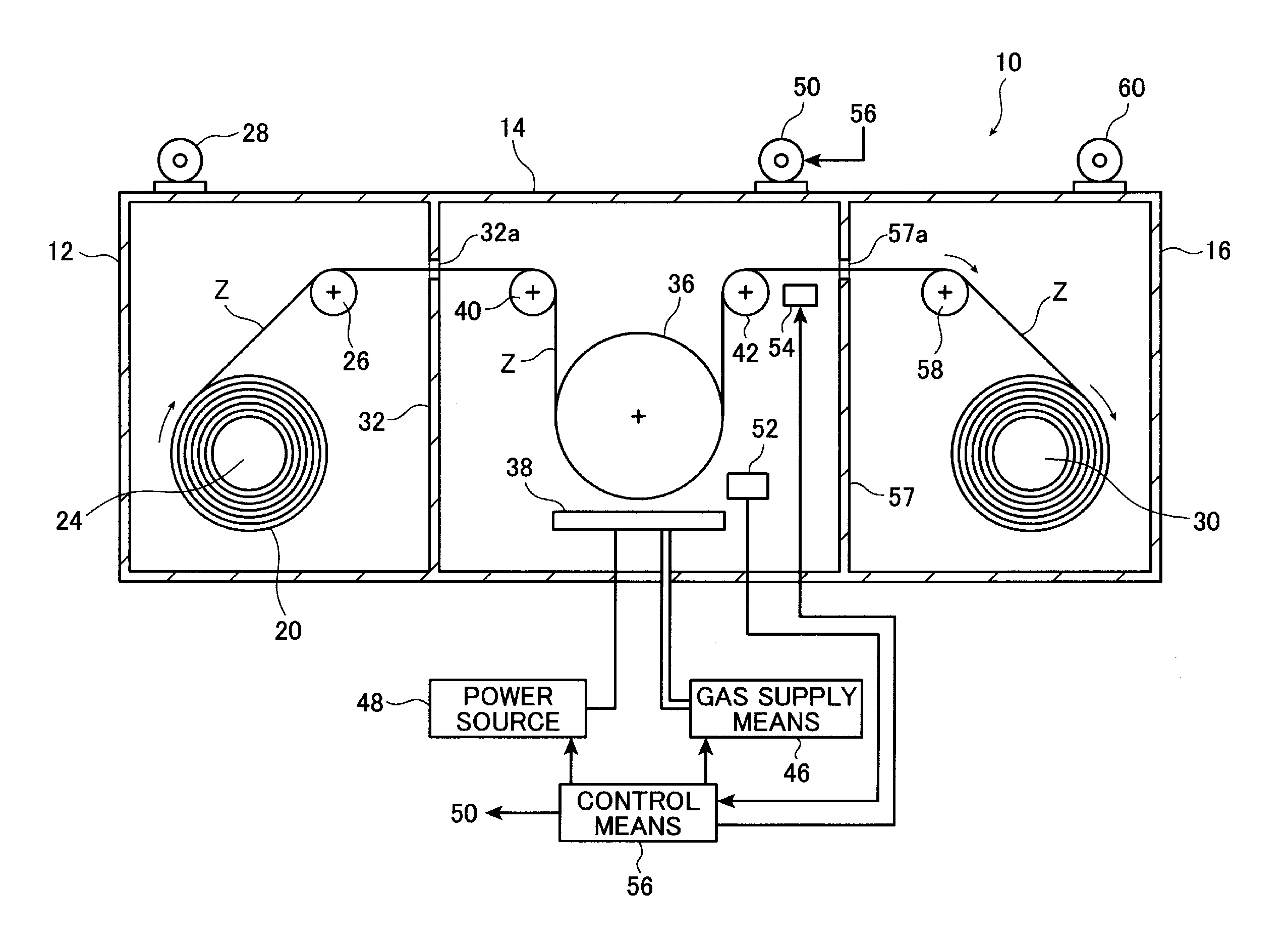
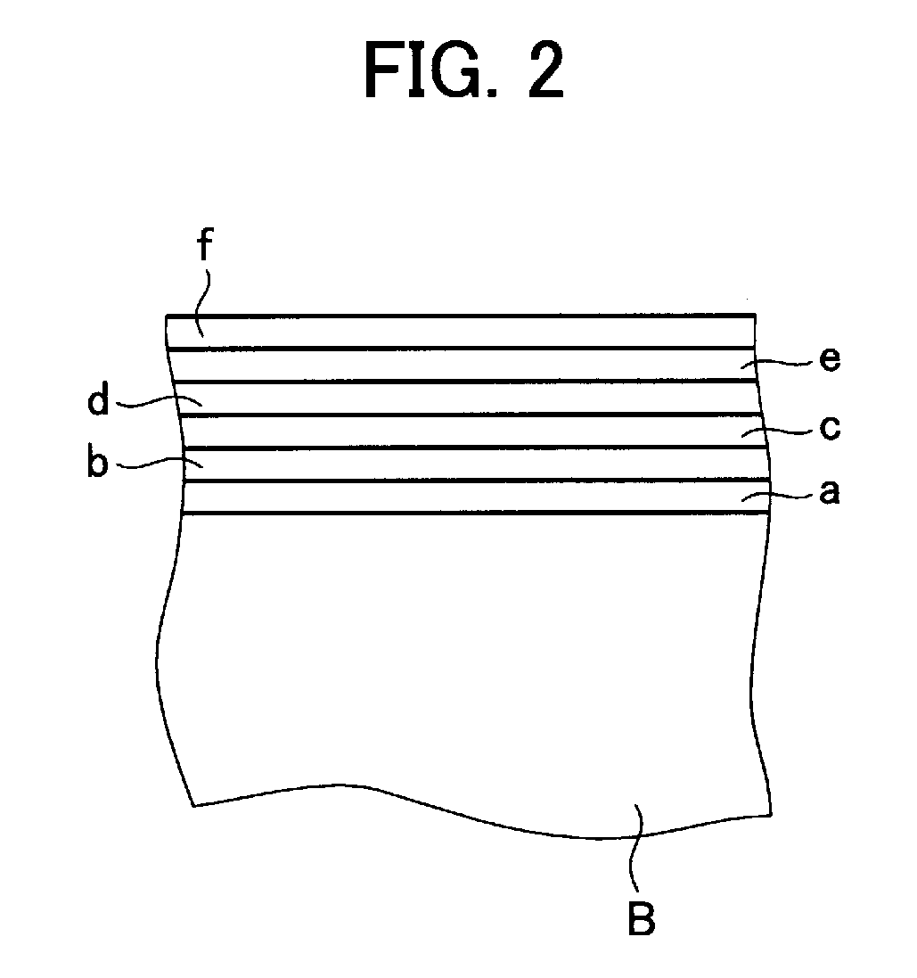
The present invention provides a gas barrier layer production method that can consistently produce a gas barrier layer with excellent gas barrier properties, transparency, and oxidation resistance. The method uses a material having at least one Si—H bond, a material having at least one N—H bond, and at least one of nitrogen, hydrogen, and a noble gas, and by forming the gas barrier layer with the plasma state controlled in accordance with emission at specified wavelengths due to generated radicals. The gas barrier layer can be used in various applications requiring high gas barrier properties, transparency, and oxidation resistance, such as displays, lighting devices, and solar batteries.

Problems solved by technology

An oxidized gas barrier layer reduces the gas barrier properties, whereby desired gas barrier properties cannot be exhibited.
However, increasingly strict requirements are recently imposed on those properties of the gas barrier layer, and some of commonly used gas barrier layers do not satisfy the required performance.
For example, the gas barrier layer of a two-sublayer structure described in US 2008 / 0211066 A1 which includes a sublayer containing a large amount of silicon and exhibiting excellent oxidation resistance can achieve excellent oxidation resistance but may often not achieve high performance in terms of transparency because of the presence of the sublayer containing a large amount of silicon.

Method used


Image

  • Method of producing gas barrier layer
  • Method of producing gas barrier layer
  • Method of producing gas barrier layer

Examples


examples

[0158]A common CVD device for depositing a film by CCP-CVD was used to form a gas barrier layer on a substrate.

[0159]The substrate used was a PET film (Lumirror T60 available from Toray Industries, Inc.; total light transmittance: 89%) with a thickness of 100 μm. The substrate had an area of 300 cm2.

[0160]A gas material including silane gas (SiH4), ammonia gas (NH3), nitrogen gas (N2) and hydrogen gas (H2) was used.

[0161]The power source used was an RF power source at a frequency of 13.56 MHz.

[0162]The substrate was set on a substrate holder in a vacuum chamber of the CVD device and the vacuum chamber was closed. Then, the vacuum chamber was evacuated and the gas material was introduced into the vacuum chamber at the point in time when the pressure dropped to 0.01 Pa.

[0163]Once the pressure in the vacuum chamber had stabilized, the plasma excitation power was supplied from the RF power source to the electrode to deposit a gas barrier layer on the substrate surface to prepare a gas b...


PUM

PropertyMeasurementUnit
temperatureaaaaaaaaaa
pressureaaaaaaaaaa

Abstract

The producing method of a gas barrier layer uses a material having at least one Si—H bond, a material having at least one N-H bond, and at least one of nitrogen gas, hydrogen gas and a noble gas and forms the gas barrier layer by plasma-enhanced CVD using a plasma in which an emission intensity A of emission at 414 nm, an emission intensity B of emission at 336 nm, an emission intensity C of emission at 337 nm, and an emission intensity D of emission at 656 nm satisfy formulas a to c:2<B / A<20  Formula aC / B<2  Formula b0.5<D / B<50.  Formula c

Description

BACKGROUND OF THE INVENTION[0001]The present invention relates to a method of producing a gas barrier layer by using plasma-enhanced CVD. More specifically, the invention relates to a gas barrier layer production method capable of depositing a gas barrier layer having not only excellent gas barrier properties but also excellent oxidation resistance and high transparency.[0002]A gas barrier layer (a water-vapor barrier layer) is formed not only on sites or parts requiring moisture resistance in various devices including optical devices, display devices (e.g. liquid-crystal displays and organic EL displays), semiconductor devices and thin-film solar batteries, but also in packaging materials used to package food, clothing, electronic components, etc.[0003]Layers made of various materials such as silicon oxide, silicon oxynitride and aluminum oxide are known gas barrier layers. A gas barrier layer made of silicon nitride is known as one of those layers. Plasma-enhanced CVD is a known m...

Claims


Application Information

Patent Timeline
Patent Type & Authority Applications(United States)
IPC IPC(8): C23C16/513C23C16/42
CPCC23C16/345C23C16/545C23C16/505
Inventor TAKAHASHI, TOSHIYA
Owner FUJIFILM CORP
Learn More