Composite substrate, elastic wave device using the same, and method for manufacturing composite substrate

Active Publication Date: 2010-09-30
NGK INSULATORS LTD
View PDF4 Cites 27 Cited by
  • Summary
  • Abstract
  • Description
  • Claims
  • Application Information

AI Technical Summary

Benefits of technology

[0007]The present invention has been conceived in consideration of the problems described above, and an object of the present invention is to provide a composite substrate which is used for an elastic wave device and which has superior heat resistance.
[0011]According to the composite substrate of the present invention, a large strain is not generated in a high-temperature treatment, and as a result, the generation of cracks is suppressed. In addition, according to the method for manufacturing a composite substrate of the present invention, the composite substrate as described above can be easily manufactured.

Problems solved by technology

However, in a conventional elastic wave device, cracks are generated in some cases after a reflow step is finished, and there has been a problem in that a production yield is low.
That is, it is believed that in the portion as described above, since a large thermal stress is generated at a high temperature due the difference in thermal expansion coefficient, a thermal strain induced by this thermal stress is increased because of the low elastic modulus, and as a result, cracks are generated.
In addition, also in a step other than the reflow step which is performed when an elastic wave device is mounted, a high-temperature process at a temperature of 250° C. to 300° C. may be performed in some cases on a composite substrate which still has a size of several inches, and in this case, cracks may also be generated by the same reason as described above.

Method used


Image

  • Composite substrate, elastic wave device using the same, and method for manufacturing composite substrate
  • Composite substrate, elastic wave device using the same, and method for manufacturing composite substrate
  • Composite substrate, elastic wave device using the same, and method for manufacturing composite substrate

Examples


example 1

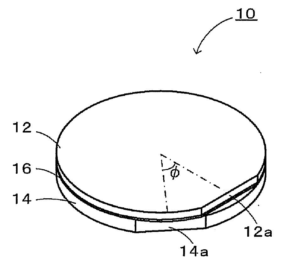
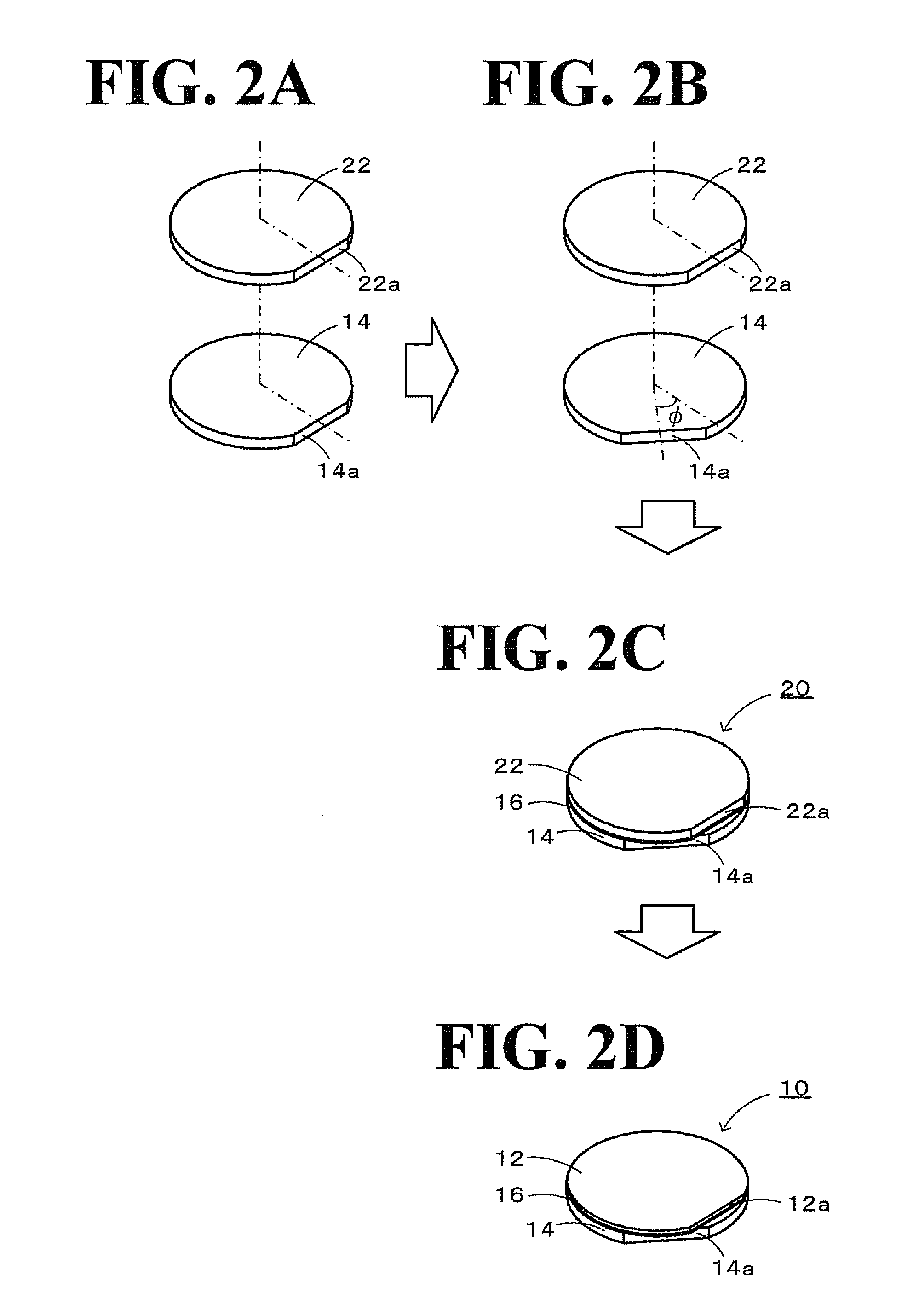
[0030]FIG. 1 is a perspective view of a composite substrate 10. This composite substrate 10 is used for a surface acoustic wave device and includes a piezoelectric substrate 12 composed of lithium tantalate (LT) capable of transmitting an elastic wave, a support substrate 14 composed of silicon and bonded to this piezoelectric substrate 12, and an adhesive layer 16 which bonds the two substrates 12 and 14. The piezoelectric substrate 12 has a thermal expansion coefficient of 16.1 ppm / K. This piezoelectric substrate 12 is a 42° Y-cut X-transmission LT substrate (42Y-X LT) that is rotated 42° from the Y axis to the Z axis about the X axis which is the transmission direction of a surface acoustic wave and has an orientation flat (hereinafter abbreviated as “orifla”) 12a. The direction of the orifla 12a of the piezoelectric substrate 12 indicates the transmission direction (X axis) of a surface acoustic wave. The support substrate 14 has a thermal expansion coefficient of 2.55 ppm / K and...

example 2

[0037]A composite substrate 10 of Example 2 was similar to that of Example 1 except that an X-cut 112° Y-transmission LT substrate (X-112Y LT) was used as the piezoelectric substrate 12. In Example 2, FIG. 6 shows the way of change in in-plane maximum thermal strain amount SH which was obtained when the above simulation (see Equation 1) was performed in which the thickness of the support substrate 14 was set to 350 μm and the thickness of the piezoelectric substrate 12 was set to 30 μm. As apparent from FIG. 6, the in-plane maximum thermal strain amount SH had the maximum value and the minimum value, and the minimum value of the in-plane maximum thermal strain amount SH was reduced by 21% to 22% as compared to the maximum value thereof.

example 3

[0038]A composite substrate 10 of Example 3 was similar to that of Example 1 except that a 128° Y-cut X-transmission lithium niobate (LN) substrate (128Y-X LN) was used as the piezoelectric substrate 12. In Example 3, FIG. 7 shows the way of change in in-plane maximum thermal strain amount SH which was obtained when the above simulation (see Equation 1) was performed in which the thickness of the support substrate 14 was set to 100 μm and the thickness of the piezoelectric substrate 12 was set to 10 μm, 20 μm, and 30 μm. As apparent from FIG. 7, the in-plane maximum thermal strain amount SH had the maximum value and the minimum value, and the minimum value of the in-plane maximum thermal strain amount SH was reduced by 10% to 11% as compered to the maximum value thereof. In addition, when the simulation was performed in a manner similar to that described above in which the thickness of the support substrate 14 was set to 200 μm and 300 μm, a graph similar to that of FIG. 7 was obtai...


PUM

PropertyMeasurementUnit
Fractionaaaaaaaaaa
Angleaaaaaaaaaa
Angleaaaaaaaaaa

Abstract

In a composite substrate 10, the piezoelectric substrate 12 which is capable of transmitting an elastic wave and a support substrate 14 which a smaller thermal expansion coefficient than the piezoelectric substrate 12 are bonded to each other. The in-plane maximum thermal strain amount which is the largest thermal strain amount in the plane of the composite substrate 10 has a minimum value and a maximum value when the piezoelectric substrate 12 and the support substrate 14 are relatively rotated 0° to 360°, and the piezoelectric substrate 12 and the support substrate 14 are bonded to each other so that the in-plane maximum thermal strain amount has the minimum value or a value in the vicinity thereof.

Description

BACKGROUND ART[0001]1. Field of the Invention[0002]The present invention relates to a composite substrate, an elastic wave device using the same, and a method for manufacturing a composite substrate.[0003]2. Description of the Related Art[0004]Hitherto, a surface acoustic wave device capable of functioning as a filter element or an oscillator used for a mobile phone or the like and an elastic wave device, such as a Lamb wave element or a thin film resonator (FBAR: Film Bulk Acoustic Resonator), using a piezoelectric thin film have been known. As the elastic wave devices described above, a device has been known which is formed in such a way that after a piezoelectric substrate which transmits an elastic wave and a support substrate having a smaller linear thermal expansion coefficient (hereinafter referred to as “thermal expansion coefficient”) than that of this piezoelectric substrate are bonded to each other to form a composite substrate having a size of several inches, many comb-t...

Claims


Application Information

Patent Timeline
IPC IPC(8): H01L41/053H01L41/18H01L41/22H01L21/02H01L41/09H01L41/187H01L41/313H03H9/25
CPCH03H3/02Y10T29/42H03H9/02574H03H9/02015
Inventor KOBAYASHI, HIROKIHORI, YUJIIWASAKI, YASUNORI
Owner NGK INSULATORS LTD
Why Eureka
Try Eureka