Nano-Scale Bridge Biosensors
a biosensor and nano-scale technology, applied in the field of nano-scale bridge biosensors, can solve the problems of changing the melting temperature, changing the thermodynamic properties, and requiring expensive fluorescent microscopes to visualize data, so as to improve the detection accuracy, reduce the cost, and improve the detection efficiency.
- Summary
- Abstract
- Description
- Claims
- Application Information
AI Technical Summary
Benefits of technology
Problems solved by technology
Method used
Image
Examples
example 1
Formation of Self-Aligned Drain / Dielectric / Source Structure (Step a in FIG. 9)
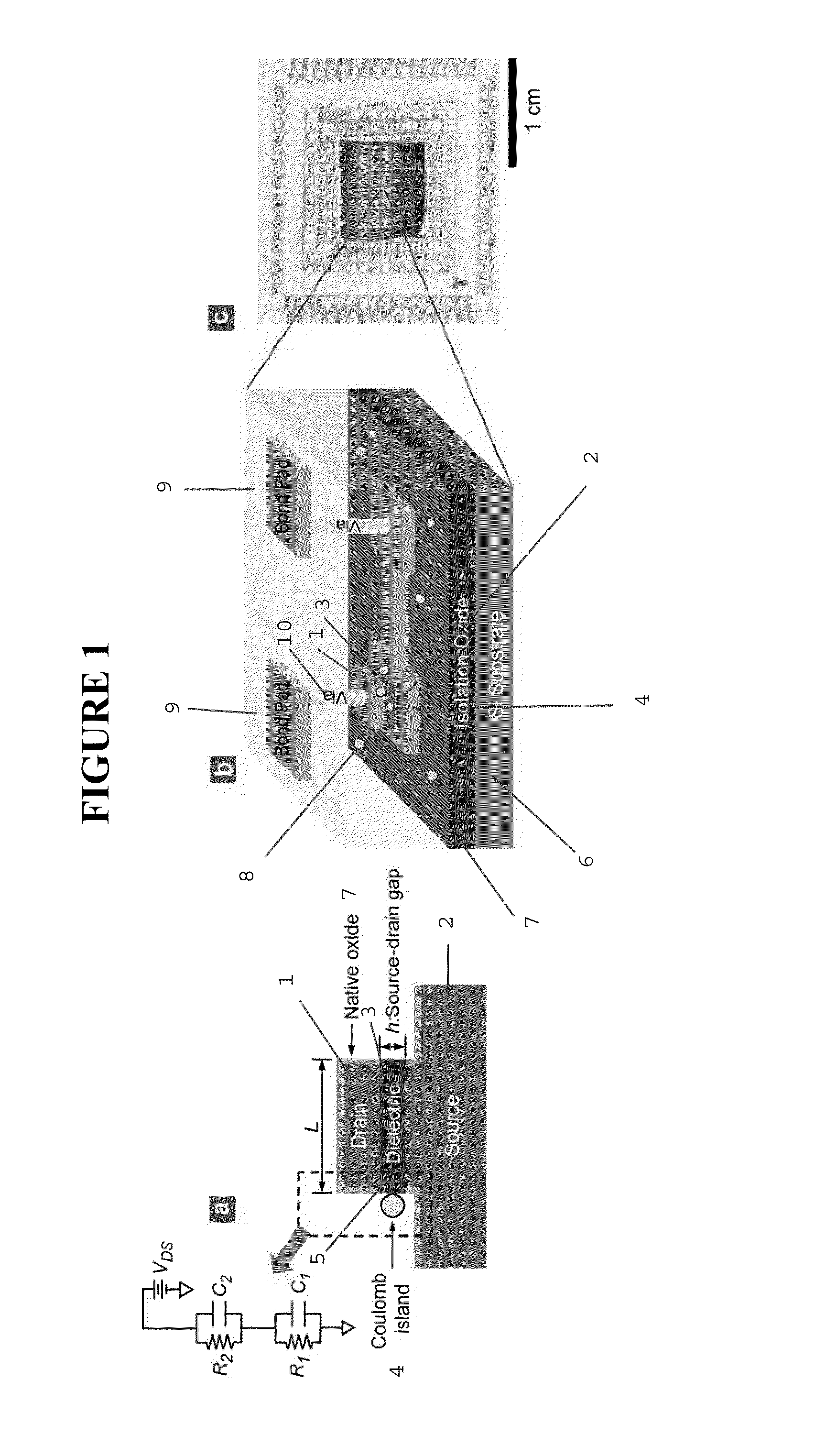
[0490]FIG. 10 displays process steps to achieve the vertically self-aligned drain / dielectric / source structure, the starting configuration in FIG. 9(a). First, a stack of films is made on a silicon wafer using standard CMOS fabrication techniques including thermal oxidation (isolation oxide), metal evaporation (source electrode 2; Au / Cr), and PECVD 3 (silicon oxide), as shown in FIG. 10(a). On top of this film stack, the drain electrode 1 (Au) is made using photolithography, evaporation of Au / Cr, and lift-off, as shown in FIG. 10(b). The lateral dimension of the drain electrode is on the order of ˜100 μm, so that the drain electrode can be easily contacted by an electrical probe during I-V measurement. Then, using the drain electrode 1 as a hard mask, the wafer is vertically etched using reactive ion etching (RIE), producing self-aligned drain / oxide / source structure, as shown in FIG. 10(a). (The PECVD oxide...
example 2
Precise Placement of the C-NPs (Step b in FIG. 9)
[0492]The next requirement is the precise placement of C-NPs along the substantially center positions of the exposed dielectric sidewall, FIG. 9(b). To achieve this, “electrostatic funneling” method is used which, as described earlier (see FIG. 3), is proven effective for placing nanoparticles on a planar surface. To demonstrate the feasibility of accurately placing C-NPs on the sensor structure, FIG. 9(b), similar three-dimensional step structures was fabricated having differing oxide thicknesses and applied the electrostatic funneling method, FIG. 11. As is clear from the scanning electron micrograph (SEM) images, nanoparticles having differing diameters (˜200, ˜80, and ˜50 nm for FIG. 11(a), (b), and (c), respectively) were placed along the center positions of the exposed oxide sidewalls. In this demonstration, the source and drain electrodes were functionalized with negatively charged SAMs (16-mercaptohexadecanoic acid; MHA) while...
example 3
Formation of Nanoparticle Satellites via DNA Hybridization (Step c in FIG. 9)
[0494]In the biosensor of the inventor, the presence of single-stranded oligonucleotide target (t-ssDNA) molecules leads to, through DNA hybridization (FIG. 9(e)), the formation of nanoparticle satellites (NP-SATs) around the C-NPs, FIG. 9(c). The important feature of the approach is that the DNA hybridization is carried out only on C-NPs. For this exclusive hybridization to be successful, it is essential that when migrating DNA molecules impinge on any surface except for that of C-NPs, they should not be adsorbed, but returned back into the solution so that they remain available for hybridization. Since DNA molecules are negatively charged, undesired adsorption can be prevented by passivating the silicon oxide surface using negatively-charged or non-polar molecules. There are a number of approaches for passivating the silicon oxide surface and forming NP-SATs around the C-NPs, such as those shown in FIG. 1...
PUM
| Property | Measurement | Unit |
|---|---|---|
| width | aaaaa | aaaaa |
| size | aaaaa | aaaaa |
| size | aaaaa | aaaaa |
Abstract
Description
Claims
Application Information
 - R&D
- Intellectual Property
- Life Sciences
- Materials
- Tech Scout
- Unparalleled Data Quality
- Higher Quality Content
- 60% Fewer Hallucinations
Browse by: Latest US Patents, China's latest patents, Technical Efficacy Thesaurus, Application Domain, Technology Topic, Popular Technical Reports.
© 2025 PatSnap. All rights reserved.Legal|Privacy policy|Modern Slavery Act Transparency Statement|Sitemap|About US| Contact US: help@patsnap.com


