Optical Article and Process for Producing the Same
a technology of optical articles and films, applied in the field of optical articles, can solve the problems of film peeling and low adhesion of gold, and achieve the effect of low sheet resistan
- Summary
- Abstract
- Description
- Claims
- Application Information
AI Technical Summary
Benefits of technology
Problems solved by technology
Method used
Image
Examples
example 1
2.1 Example 1
Sample S1
2.1.1 Selection of Lens Base Material and Formation of Hard Coat Layer
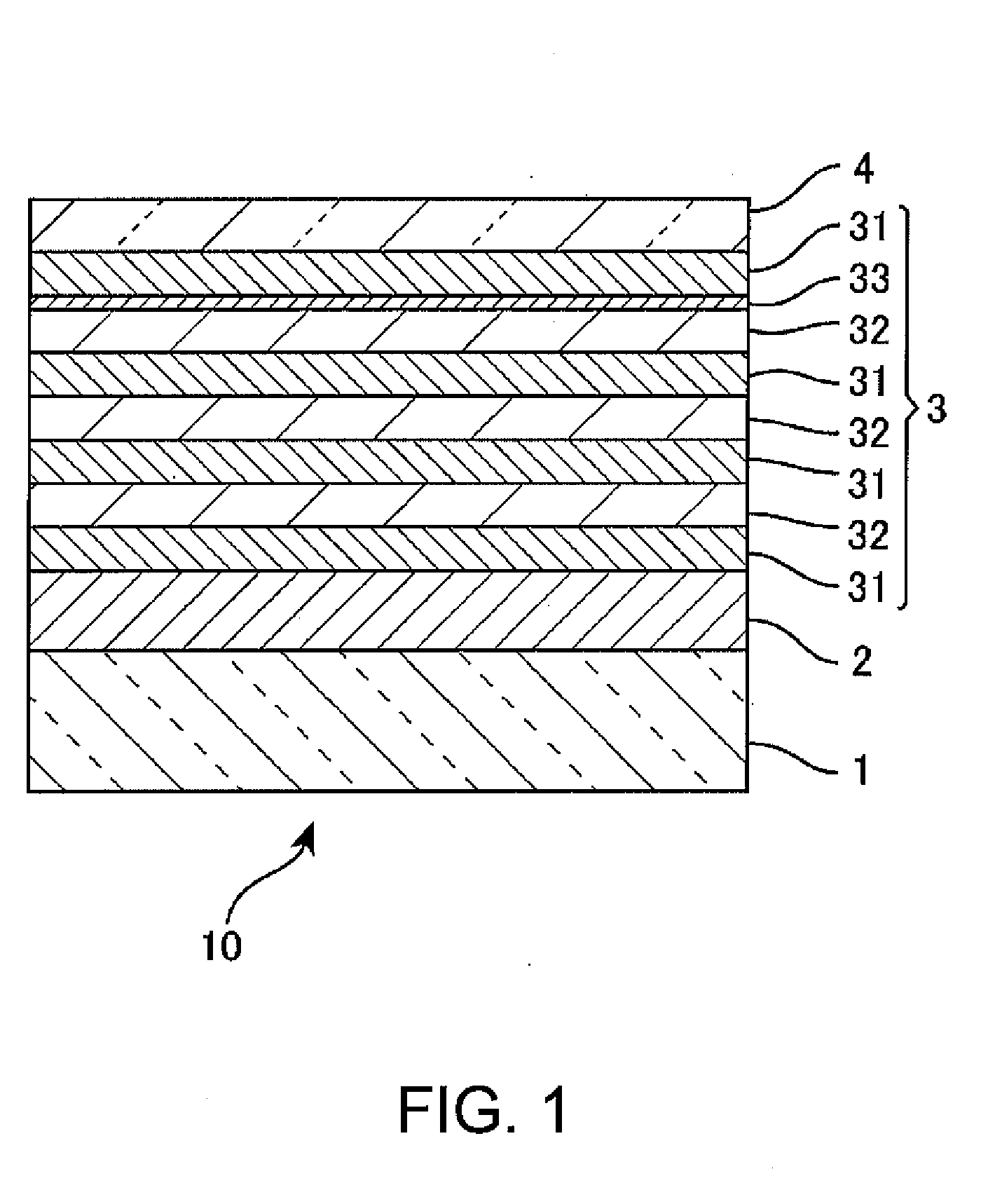
[0049]As a lens base material 1, a plastic lens base material for spectacles (manufactured by Seiko Epson Corporation, trade name: Seiko Super Sovereign (SSV)) having a refractive index of 1.67 was used.
[0050]An application liquid (coating liquid) for forming a hard coat layer 2 was prepared as follows. In 20 parts by weight of Epoxy Resin / Silica Hybrid (trade name: Compoceran (registered trademark) E102 (manufactured by Arakawa Chemical industries, Ltd.)), 4.46 parts by weight of an acid anhydride-based curing agent (trade name: liquid curing agent (C2) (manufactured by Arakawa Chemical industries, Ltd.)) was mixed and stirred, whereby an application liquid (coating liquid) was obtained. This coating liquid was applied on the lens base material 1 to a predetermined thickness using a spin coater, whereby the hard coat layer 2 was formed. The lens base material after application was baked at 1...
example 2
2.2 Example 2
Sample S2
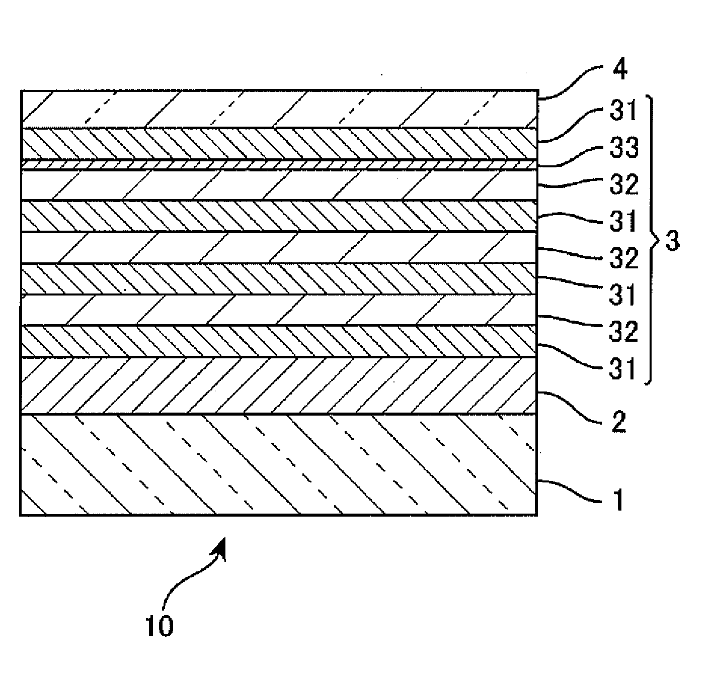
[0069]In Example 2, a transparent white plate glass (B270) was used as a lens base material 1, and an antireflection layer 3 was formed directly on the lens base material 1 without forming a hard coat layer 2 by alternately laminating a silicon dioxide (SiO2) layer as a low refractive index layer 31 and a titanium oxide (TiO2) layer as a high refractive index layer 32 under the same film forming conditions as in Example 1. The first layer, third layer, fifth layer, and eight layer were each the low refractive index layer 31, and the second layer, fourth layer, and sixth layer were each the high refractive index layer 32. Further, a conductive layer 33 was formed as the seventh layer under the same film forming conditions as in Example 1. Moreover, an antifouling layer 4 was formed on the antireflection layer 3.
examples 3 and 4
2.3 Examples 3 and 4
Lens Sample S3 and Glass Sample S4
[0070]Sample 53 using a plastic lens as a lens base material 1 and Sample S4 using a white plate glass as a lens base material 1 were produced in the same manner as in Example 1 and Example 2, respectively. However, the film forming conditions for a conductive layer 33 were changed as follows.[0071]Film forming conditions for conductive layer 33[0072]Underside layer (primary layer): TiO2 [0073]Vapor source: Metal Ge[0074]Film formation rate: 0.1 nm / sec[0075]Vapor time: 10 sec[0076]Ion-assisted vapor: With[0077]Ion energy: 500 eV (Gas species; argon, Beam current: 150 mA, Bias current: 250 mA)
PUM
| Property | Measurement | Unit |
|---|---|---|
| refractive index | aaaaa | aaaaa |
| temperature | aaaaa | aaaaa |
| refractive index | aaaaa | aaaaa |
Abstract
Description
Claims
Application Information
 - R&D
- Intellectual Property
- Life Sciences
- Materials
- Tech Scout
- Unparalleled Data Quality
- Higher Quality Content
- 60% Fewer Hallucinations
Browse by: Latest US Patents, China's latest patents, Technical Efficacy Thesaurus, Application Domain, Technology Topic, Popular Technical Reports.
© 2025 PatSnap. All rights reserved.Legal|Privacy policy|Modern Slavery Act Transparency Statement|Sitemap|About US| Contact US: help@patsnap.com


