Method for etching a layer on a silicon semiconductor substrate

Inactive Publication Date: 2010-08-12
ROBERT BOSCH GMBH
View PDF5 Cites 187 Cited by
  • Summary
  • Abstract
  • Description
  • Claims
  • Application Information

AI Technical Summary

Benefits of technology

[0007]The method according to the present invention for etching an SiGe mixed semiconductor layer on a silicon semiconductor substrate by dry chemical etching of the SiGe mixed semiconductor layer with the aid of an etching gas selected from the group that includes ClF3 and / or ClF5 has the advantage that increased selectivity of etching silicon-germanium with respect to silicon may be provided in the dry chemical etching process.
[0008]This makes it possible to expose existing silicon structures or functional dielectric layers using reduced or even no further protective measures by etching silicon-germanium sacrificial layers. It is advantageous that silicon-germanium may be selectively etched, without passivation of silicon function structures being necessary.
[0011]It was surprisingly found that the addition of chlorine and / or HCl to the etching gas at unchanged partial pressure of the etching gas causes a reduced etching attack on silicon without disadvantageously affecting the etching rate of silicon-germanium. By reducing undesired etching of silicon compared to silicon-germanium, the method according to the present invention makes sacrificial layer etching possible, which allows even thinner or more critically dimensioned silicon functional elements to be manufactured. This allows previously critical design geometries to be manufactured; in particular, further reduced micromechanical structures, in particular sensor structures, may be exposed.
[0012]It is of particular advantage that sacrificial layers, for example, of silicon-germanium, may be removed without noticeably etching functional structural elements of silicon or other functional, silicon-based layers such as silicon nitride or silicon oxide.
[0013]The increased selectivity achievable via the method according to the present invention advantageously allows greater undercut widths to be achieved. Furthermore, the method according to the present invention makes it possible to increase the etching rate of silicon-germanium, for example, via higher process pressures, without silicon structural elements being noticeably attacked, thanks to the higher selectivity of the method. This makes further improved undercut widths and / or shortened process times possible.
[0014]It is highly advantageous that, in particular, very small or very narrow or even very extended planar silicon structures may be exposed, since rapid and very selective etching may be provided.

Problems solved by technology

The disadvantage of the known etching processes is that the achievable selectivity of etching silicon-germanium with respect to silicon limits the manufacture of complex structures and geometries by semiconductor technology using controlled removal of materials, in particular controlled removal of sacrificial layers, for example, in layer stacks, in the manufacturing processes of semiconductor components.

Method used


Image

  • Method for etching a layer on a silicon semiconductor substrate
  • Method for etching a layer on a silicon semiconductor substrate

Examples


Embodiment Construction

[0017]The method according to the present invention is first elucidated as an example in connection with in-situ production of ClF3.

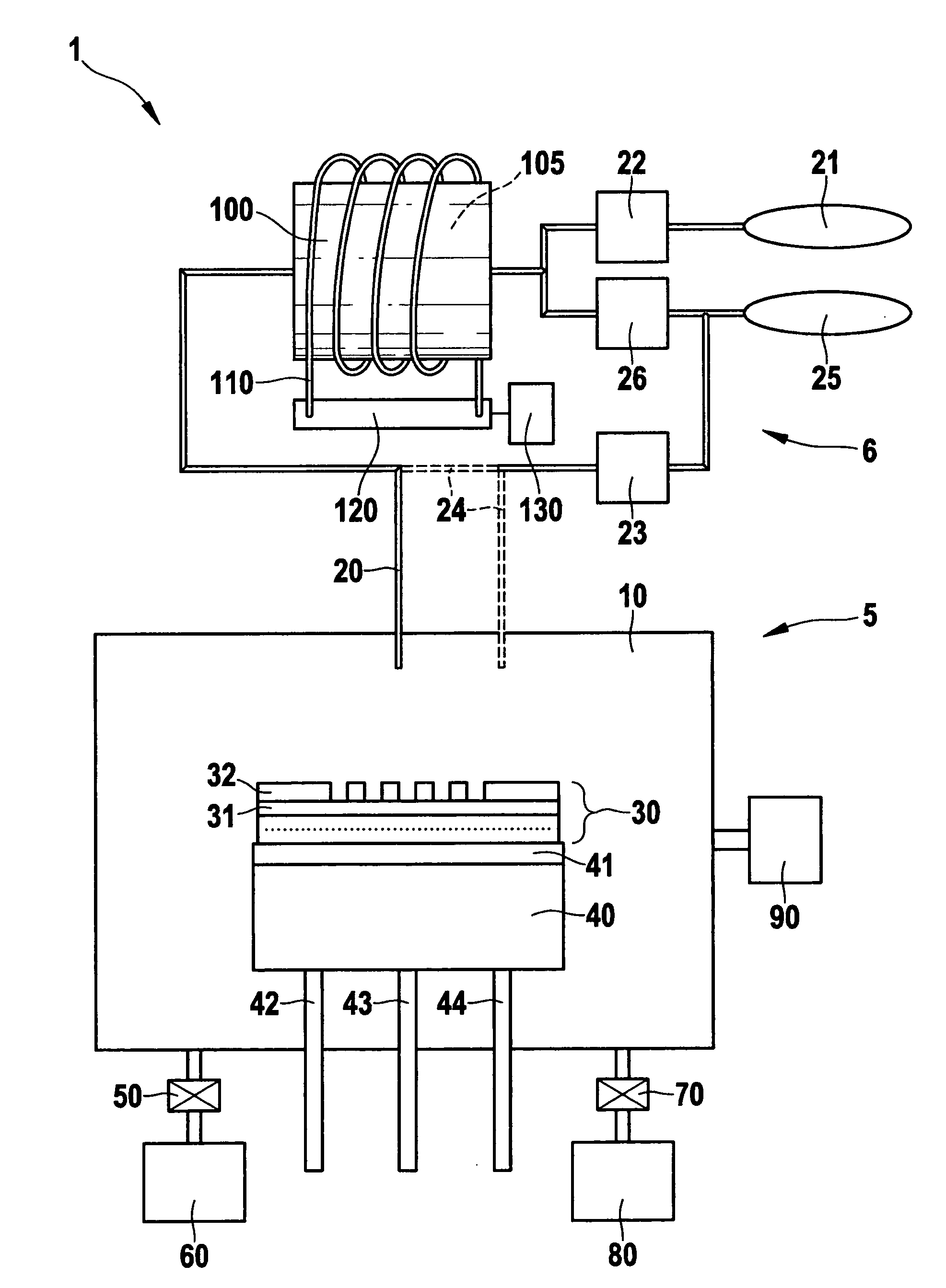
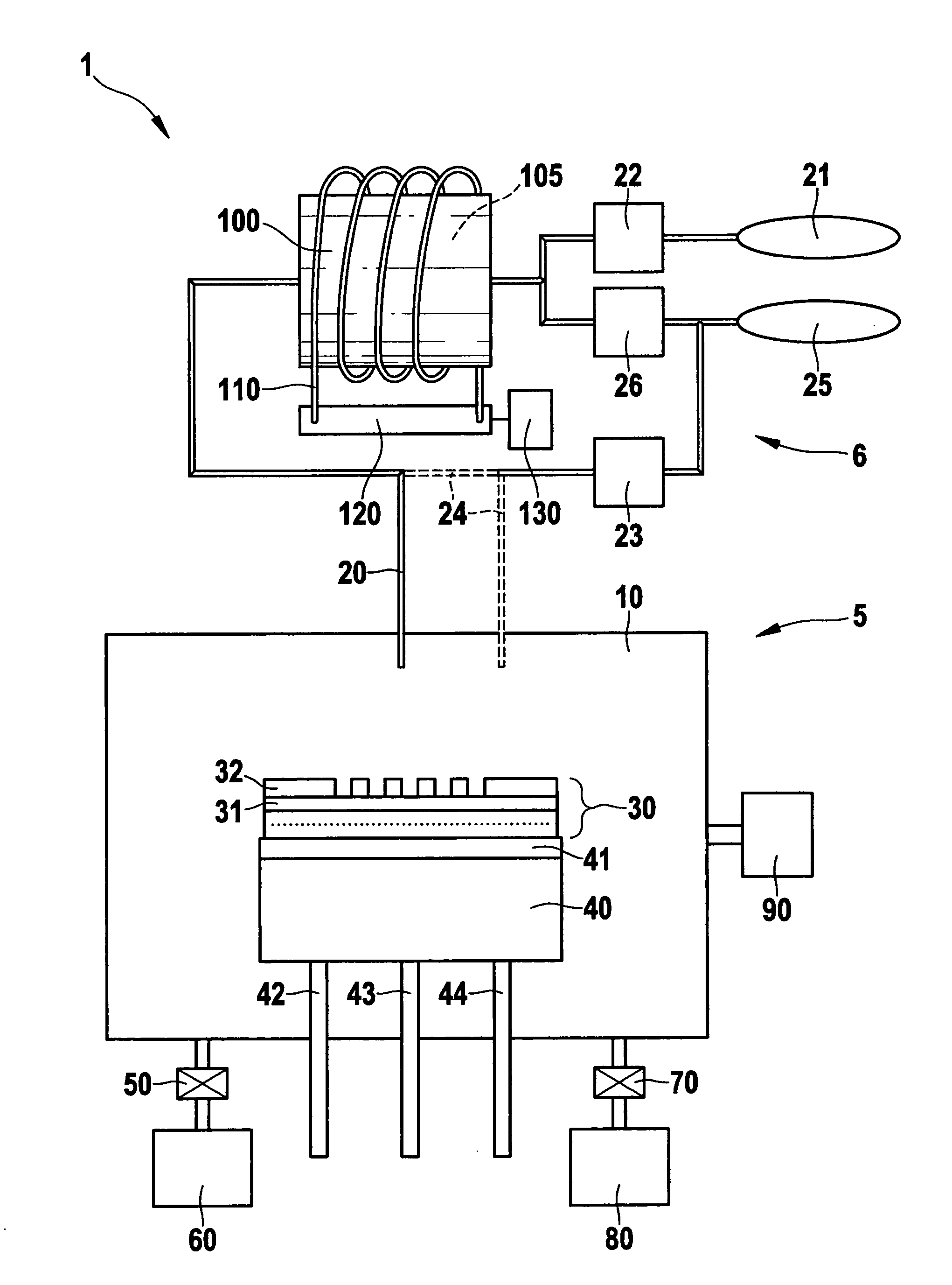
[0018]FIG. 1 shows a device 1 including an etching system 5, which has a process chamber 10 in which a semiconductor substrate 30, which may be a silicon wafer having a silicon-germanium mixed semiconductor layer 31, is etched. Etching system 5 is provided with a device 6 for generating chlorine trifluoride (ClF3). Systems associated with devices for generating chlorine trifluoride are disclosed in Patent Specification DE 102 29 037 A1 to which reference is hereby made. The system discussed in Patent Specification DE 102 29 037 A1 and provided with a device for generating chlorine trifluoride differs from the system disclosed according to the exemplary embodiments and / or exemplary methods of the present invention in that no arrangement is provided which would permit additionally adding gases selected from the group including Cl2 and / or HCl to the etchin...


PUM

PropertyMeasurementUnit
Pressureaaaaaaaaaa
Pressureaaaaaaaaaa
Pressureaaaaaaaaaa

Abstract

A method for selective etching of an SiGe mixed semiconductor layer on a silicon semiconductor substrate by dry chemical etching of the SiGe mixed semiconductor layer with the aid of an etching gas selected from the group including ClF3 and / or ClF5, a gas selected from the group including Cl2 and / or HCl being added to the etching gas.

Description

FIELD OF THE INVENTION[0001]The present invention relates to a method for etching an SiGe mixed semiconductor layer on a silicon semiconductor substrate by dry chemical etching.BACKGROUND INFORMATION[0002]In manufacturing semiconductor components, in particular in manufacturing cantilevered sensor structures by surface micromechanical technology, selective removal of a certain layer, a so-called sacrificial layer, selectively with respect to the functional layer, is an often necessary measure. Such a sacrificial layer may be removed, in principle, by dry chemical or wet chemical methods. Sacrificial layers are preferably removed with the aid of gaseous etching media, since when using etching gases, the risk of irreversible adhesion of sensor structure elements to the silicon substrate thereunder or of parts of the sensor structure elements to each other, the so-called sticking risk, is considerably reduced or eliminated.[0003]In manufacturing micromechanical structures or components...

Claims


Application Information

Patent Timeline
IPC IPC(8): H01L21/306C23F1/08
CPCB81C1/00531B81C1/00595B81C2201/0132H01L21/02019H01L21/3065H01L21/32135H01L21/30621B81C2201/0138
Inventor BECKER, VOLKERLAERMER, FRANZFUCHS, TINOLEINENBACH, CHRISTINA
Owner ROBERT BOSCH GMBH
Why Eureka
Try Eureka