
Semiconductor memory device and reading method therefor

a memory device and semiconductor technology, applied in the direction of information storage, static storage, digital storage, etc., can solve the problems of long charging period of bit lines, capacitance contact, and only accessing at medium speed, so as to reduce the noise of the charge voltage generating circuit and high speed

Inactive Publication Date: 2010-08-05
ELPIDA MEMORY INC
View PDF8 Cites 32 Cited by
  • Summary
  • Abstract
  • Description
  • Claims
  • Application Information

AI Technical Summary

Benefits of technology

[0020]According to the embodiment, the bit line and the reference bit line are charged to the initial voltage by using the charge that is charged to a voltage higher than the initial voltage. The charges that are charged to high voltage are distributed to the bit line and the reference bit line for performing charge sharing, and hence the bit line and the reference bit line can be charged to the initial voltage at high speed. Because the bit line and the reference bit line can be charged to the initial voltage at high speed, the device can be read at high speed. In addition, the charges that are charged to high voltage can be prepared in sufficient time in the charge voltage generating circuit except for a period for charging the bit line and for reading out information. Therefore, maximum current in the charge voltage generating circuit can be controlled, and noise due to the charge voltage generating circuit can be reduced compared with the case where the constant voltage power supply is used.

Problems solved by technology

In contrast, the non-volatile memory has an advantage that it can maintain the stored information even if power supply is turned off, but has a disadvantage that it can be accessed only at medium speed and cannot be accessed at random.
Therefore, if the memory element is a high resistance element, there is a problem that charging of the parasitic capacitance contact is so slow that charging period of the bit line becomes long.
In addition, if several tens of thousands of bit lines are read simultaneously by the same number of sense amplifiers in the array, there are problems that the supply capability of the constant voltage generating source is decreased because of large current consumption and that noise is generated on the GND potential due to a parasitic resistance of wiring or other factors.

Method used


Image

  • Semiconductor memory device and reading method therefor
  • Semiconductor memory device and reading method therefor
  • Semiconductor memory device and reading method therefor

Examples


Embodiment Construction

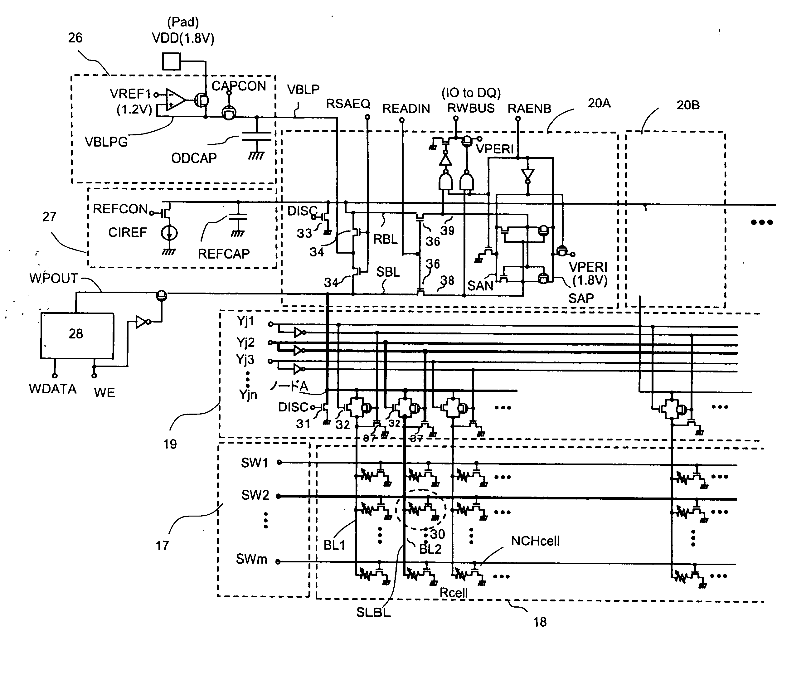
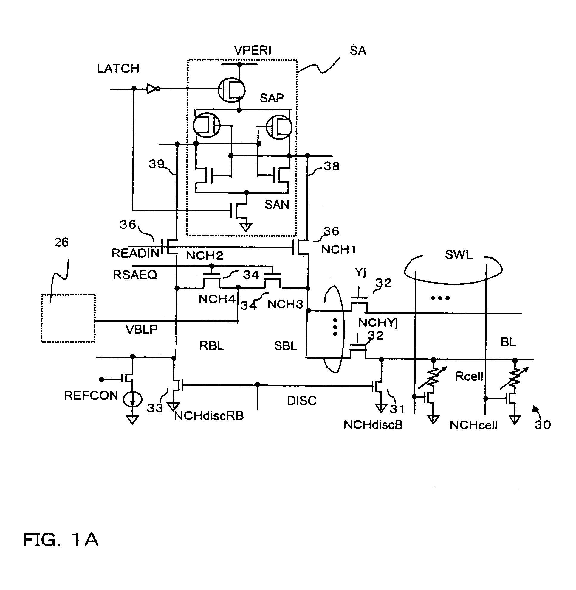
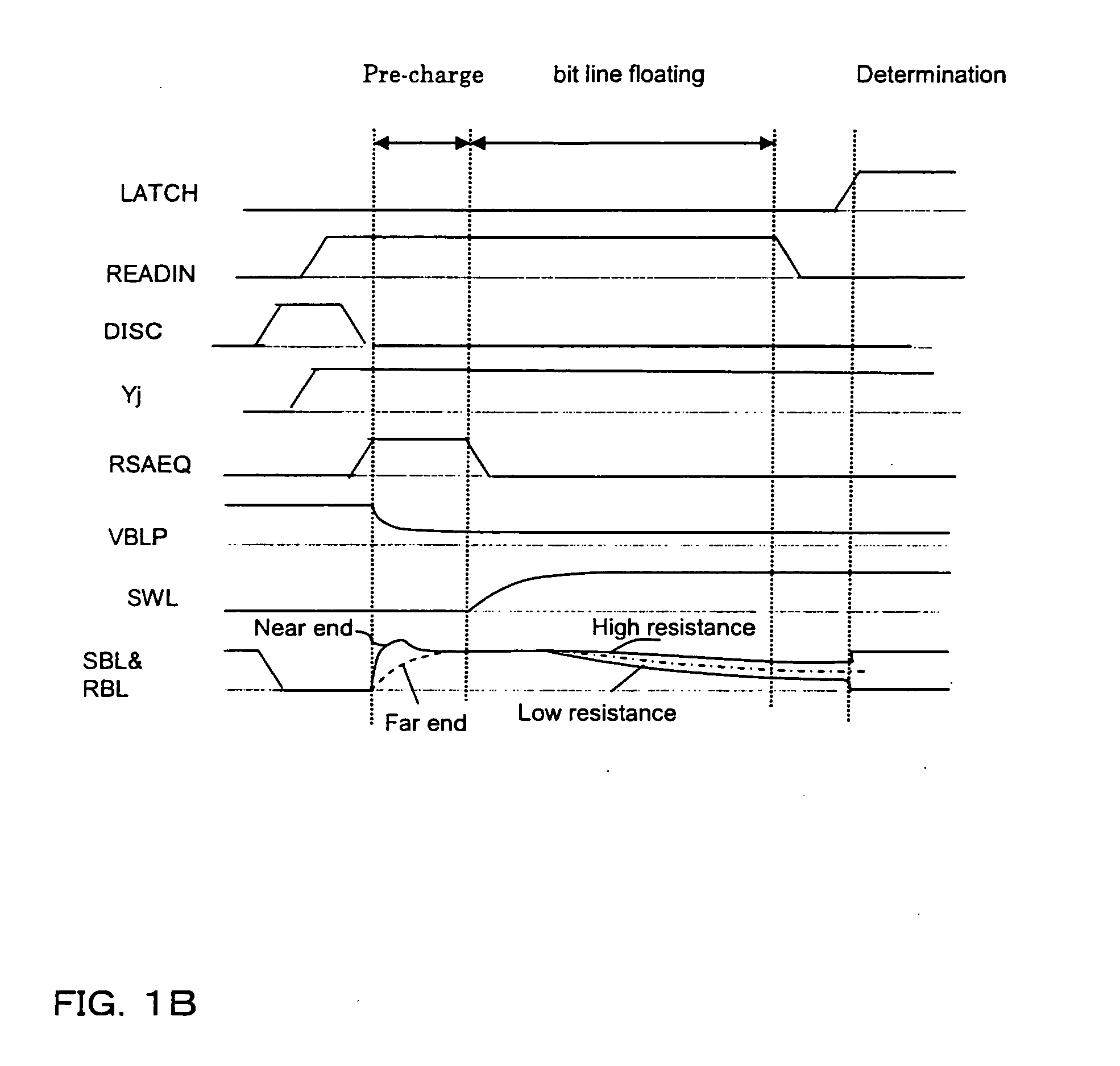
[0033]An embodiment of the present invention is described in detail with reference to the attached drawings. FIGS. 1A and 1B are a schematic structural diagram for illustrating a basic structure of a semiconductor memory device according to the embodiment of the present invention and a read timing chart thereof, respectively. FIG. 2 is a general structure diagram of the semiconductor memory device, FIG. 3 is a detailed block diagram thereof, and FIG. 4 is a read timing chart thereof. FIG. 5 is a circuit diagram of a bit line charge voltage generating circuit that is used in the embodiment, FIGS. 6A and 6B are diagrams illustrating layouts of the bit line charge voltage generating circuit and wirings of a power supply respectively in a bank and a mat of the semiconductor memory device. FIG. 7 illustrates a write timing chart of the semiconductor memory device according to the embodiment.

[0034]In FIG. 1A, the basic structure includes memory cells 30 (Rcell and NCHcell), bit line selec...


PUM


Abstract

A memory device is configured such that, in a read access: a first switch and a second switch are turned on in a pre-charge period before a memory cell is accessed so that charges of a bit line charge voltage generating circuit are distributed to a bit line and a reference bit line, to thereby charge the bit line and the reference bit line to an initial voltage. After the charge, a selected memory cell is connected to the bit line, the reference bit line is connected to a reference voltage generating circuit, and a voltage differential type sense amplifier amplifies a difference voltage between a voltage of the bit line decreased by discharge of the selected memory cell and a voltage of the reference bit line generated by the reference voltage generating circuit, to thereby read out memory cell data.

Description

[0001]This application is based upon and claims the benefit of priority from Japanese patent application No. 2009-023248, filed on Feb. 4, 2009, the disclosure of which is incorporated herein in its entirety by reference.BACKGROUND OF THE INVENTION[0002]1. Field of the Invention[0003]The present invention relates to a semiconductor memory device, and more particularly, to a semiconductor memory device capable of being read at high speed and a reading method therefor.[0004]2. Description of the Related Art[0005]There are two types of semiconductor memory devices, that is, a volatile memory which does not retain stored information if power supply is turned off, and a non-volatile memory which retains the stored information even if power supply is turned off. For instance, a dynamic random access memory (DRAM) and a static random access memory (SRAM) are volatile memories while an electrically erasable programmable read only memory (EEPROM) and a flash memory are non-volatile memories....

Claims


Application Information

Patent Timeline
Patent Type & Authority Applications(United States)
IPC IPC(8): G11C5/14G11C7/02G11C7/00
CPCG11C5/145G11C7/12G11C7/02G11C5/147G11C11/1673G11C11/1693
Inventor SEKO, AKIYOSHI
Owner ELPIDA MEMORY INC
Learn More