Organic transistor, organic transistor array, and display device

a technology of organic transistors and display devices, applied in semiconductor devices, solid-state devices, thermoelectric devices, etc., can solve the problems of increased power consumption, degraded transistor properties, crosstalk when displaying pixels, etc., and achieve the effect of decreasing the off curren

Active Publication Date: 2010-08-05
RICOH KK
View PDF2 Cites 17 Cited by
  • Summary
  • Abstract
  • Description
  • Claims
  • Application Information

AI Technical Summary

Benefits of technology

[0025]According to one embodiment of the present invention, there are provided an organic transistor capable of decreasing the off current while the transistor is operating, an organic transistor array including a plurality of such organic transistors, and a display device including the organic transistor array.

Problems solved by technology

If the organic TFT is integrated without forming a pattern of the organic semiconductor layer, the following problem may occur.
That is, due to the impact of the organic semiconductor layer formed on portions other than the channel region, an off current may be generated while the transistor is operating, in which case power consumption will increase.
Furthermore, this may cause crosstalk when displaying pixels.
However, when a high polymer material is used as the organic semiconductor material, and a pattern is formed by applying a photoresist on the high polymer material, the transistor properties may be degraded.
Furthermore, damage may be caused by using a peeling agent such as ethylene glycol monobutyl ether and monoethanolamine when peeling off the resist.
Damage may be caused by rinsing the organic semiconductor layer with pure water after peeling off the resist.
Due to the above reasons, it is difficult to form a pattern of the organic semiconductor layer by the conventional photolithography etching method.
However, the problem with these processes is that as the number of process steps increases, the throughput will decrease and the manufacturing cost will increase.
However, with this method, the organic semiconductor material is limited, and therefore the freedom in selecting the material is low.
However, when forming a pattern on a large area, it is difficult to perfectly form a pattern for all transistors, due to factors such as the precision in points of impact.
Thus, it is difficult to adjust the physical properties to appropriate levels.
For this reason, ink cannot always be jetted properly from all of the nozzles.
As a result, the organic semiconductor layer may be a partially incomplete pattern.
Such a problem is particularly notable when forming patterns on a large area.

Method used


Image

  • Organic transistor, organic transistor array, and display device
  • Organic transistor, organic transistor array, and display device
  • Organic transistor, organic transistor array, and display device

Examples


example 1

Practical Example 1

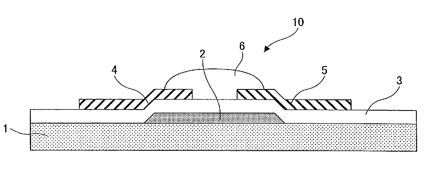
[0063]By performing a vacuum deposition method using a shadow mask, an adherence layer (not shown) made of Cr having a film thickness of 3 nm and the gate electrode 2 made of Al having a film thickness of 100 nm were formed on the glass substrate 1. Next, by performing a CVD method, the gate insulating film 3 made of polyparaxylylene having a film thickness of 500 nm obtained from a di-monochloro-paraxylylen solid dimer was formed on the gate electrode 2. Furthermore, by performing a vacuum deposition method using a shadow mask, patterns of the source electrode 4 and the drain electrode 5 made of Au having film thicknesses of 50 nm were formed on the gate insulating film 3. The channel width was 140 μm and the channel length was 10 μm. Next, the inkjet method was performed to print the organic semiconductor layer 6 in an island-like shape with the use of a solution made of a material expressed by the chemical formula (A), on the gate insulating film 3 having the s...

example 2

Practical Example 2

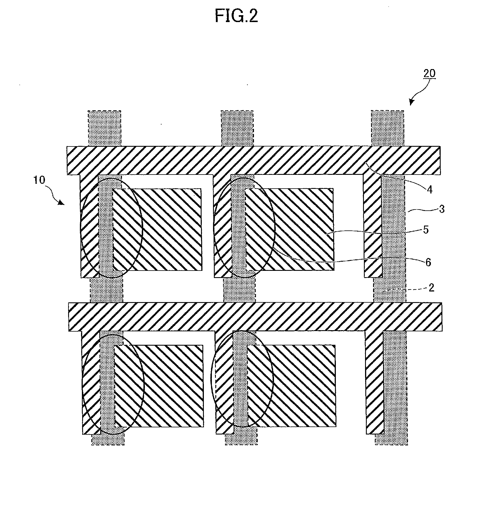
[0068]The organic semiconductor layers 6 were formed as stripes on the gate insulating film 3 with the source electrode 4 and the drain electrode 5 formed thereon. Otherwise, the organic transistor array 30 was obtained in the same manner as that of practical example 1.

[0069]Next, the on current and the off current were measured in the same manner as that of practical example 1. The on current Ids was −4.66×10⁻⁸ A (Vg=−20 V), the off current Ids was −3.81×10⁻¹¹ A (Vg=+20 V), and the on / off ratio (Vg=−20 V / Vg=+20 V) was 1.22×10³.

example 3

Practical Example 3

[0073]The organic semiconductor layer 6 was formed, by a spin-coating method, over the entire the gate insulating film 3 with the source electrode 4 and the drain electrode 5 formed thereon. Otherwise, the organic transistor array 40 was obtained in the same manner as that of practical example 1.

[0074]Next, the on current and the off current were measured in the same manner as that of practical example 1. The on current Ids was −3.76×10⁻⁸ A (Vg=−20 V), the off current Ids was −4.55×10⁻¹⁰ A (Vg=+20 V), and the on / off ratio (Vg=−20 V / Vg=+20 V) was 8.26×10.


PUM


Abstract

An organic transistor includes a substrate; a gate electrode and a gate insulating film sequentially formed on the substrate in the stated order; and a source electrode, a drain electrode, and an organic semiconductor layer formed on at least the gate insulating film. Ultraviolet light is radiated to the substrate from a side without the gate electrode, transmitted through the substrate and the gate insulating film, reflected at the gate electrode, and absorbed at the organic semiconductor layer. Conductivity of the organic semiconductor layer that has absorbed the ultraviolet light is lower than that of the organic semiconductor layer that has not absorbed the ultraviolet light.

Description

TECHNICAL FIELD[0001]The present invention relates to an organic transistor, an organic transistor array, and a display device.BACKGROUND ART[0002]Active research is being conducted for organic thin-film transistors (TFTs), as they have the following advantages.[0003]1. High flexibility in terms of the variety in the materials, manufacturing method, and product format.[0004]2. The area can be easily increased.[0005]3. The layer structure can be simplified, and the manufacturing process can be simplified.[0006]4. A low-cost manufacturing device can be used for the manufacturing process.[0007]Examples of the film forming method of the organic semiconductor layer are a printing method, a spin-coating method, and a dipping method. An organic TFT can be manufactured at a considerably lower cost compared to a conventional TFT using a Si semiconductor material.[0008]When integrating an organic TFT, it is necessary to form an electrode pattern. Patent document 1 discloses a method of manufa...

Claims


Application Information

Patent Timeline
Patent Type & Authority Applications(United States)
IPC IPC(8): H01L51/50H01L51/10
CPCH01L27/283H01L51/0558H01L51/0022H01L51/0015H10K19/10H10K71/135H10K71/211H10K71/611H10K10/484H10K71/40
Inventor YUTANI, KEIICHIROTOMONO, HIDENORIYAMAGA, TAKUMI
Owner RICOH KK
Why Eureka
Try Eureka