
Integrated circuit device with single crystal silicon on silicide and manufacturing method

a technology of integrated circuit devices and silicides, applied in semiconductor devices, semiconductor/solid-state device details, diodes, etc., can solve problems such as parasitic devices, breakdown or current leakage, and utilization of silicides

Active Publication Date: 2010-07-08
MACRONIX INT CO LTD
View PDF21 Cites 18 Cited by
  • Summary
  • Abstract
  • Description
  • Claims
  • Application Information

AI Technical Summary

Benefits of technology

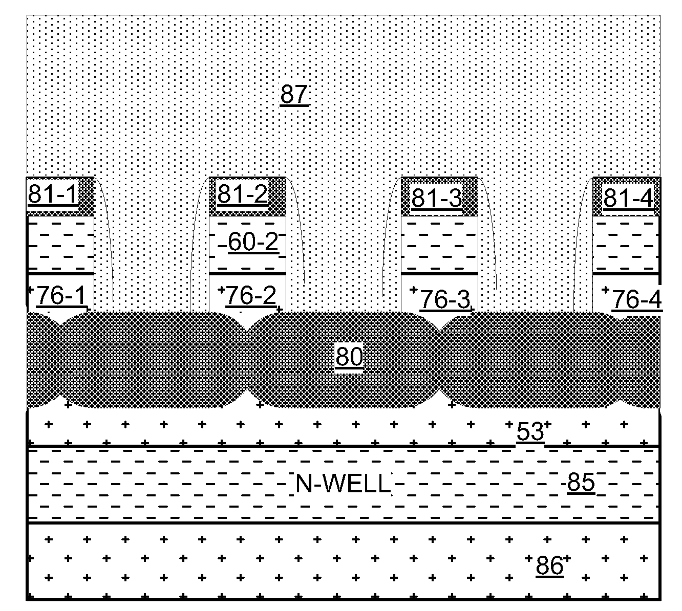
[0011]In an embodiment of the manufacturing method described herein, a sidewall blocking layer is formed on the sides of the protruding element, and an etching step is executed, which etches into the single crystal silicon body using the sidewall blocking layer as a mask to expose a portion of the single crystal silicon body beneath the sidewall blocking layer. The portions of the single crystal silicon body beneath the sidewall blocking layer are consumed by the silicide formation, while the blocking layer protects the upper portions of the protruding element from silicide formation. Thereby, the upper portion of the protruding element remains in a single crystal state, and becomes separated from the underlying single crystal silicon body by the silicide formed beneath it. The silicide made using this process is integral with the underlying silicon body and the overlying silicon node, in the sense that the formation silicide by consuming the silicon integrates the silicide within the protruding elements. This integral nature of the silicide provides a silicon / silicide interface with excellent electrical and structural characteristics.

Problems solved by technology

A problem that arises with the use of buried diffusion lines or other doped semiconductor features is the formation of parasitic devices.
These carriers can migrate into the buried diffusion lines, and activate parasitic devices causing breakdown or current leakage.
One limitation on the utilization of silicides arises because there is no practical technique for providing a single crystal silicon node on top of a silicide, or for providing a silicide between two single crystal nodes of silicon, without intervening layers of material.
Thus, certain types of devices in which it is preferable to utilize single crystal silicon cannot be formed on top of a silicide contact.
This limitation arises in the formation of vertical access devices such as diodes and transistors in memory arrays, and in other vertical device structures.

Method used


Image

  • Integrated circuit device with single crystal silicon on silicide and manufacturing method
  • Integrated circuit device with single crystal silicon on silicide and manufacturing method
  • Integrated circuit device with single crystal silicon on silicide and manufacturing method

Examples


Embodiment Construction

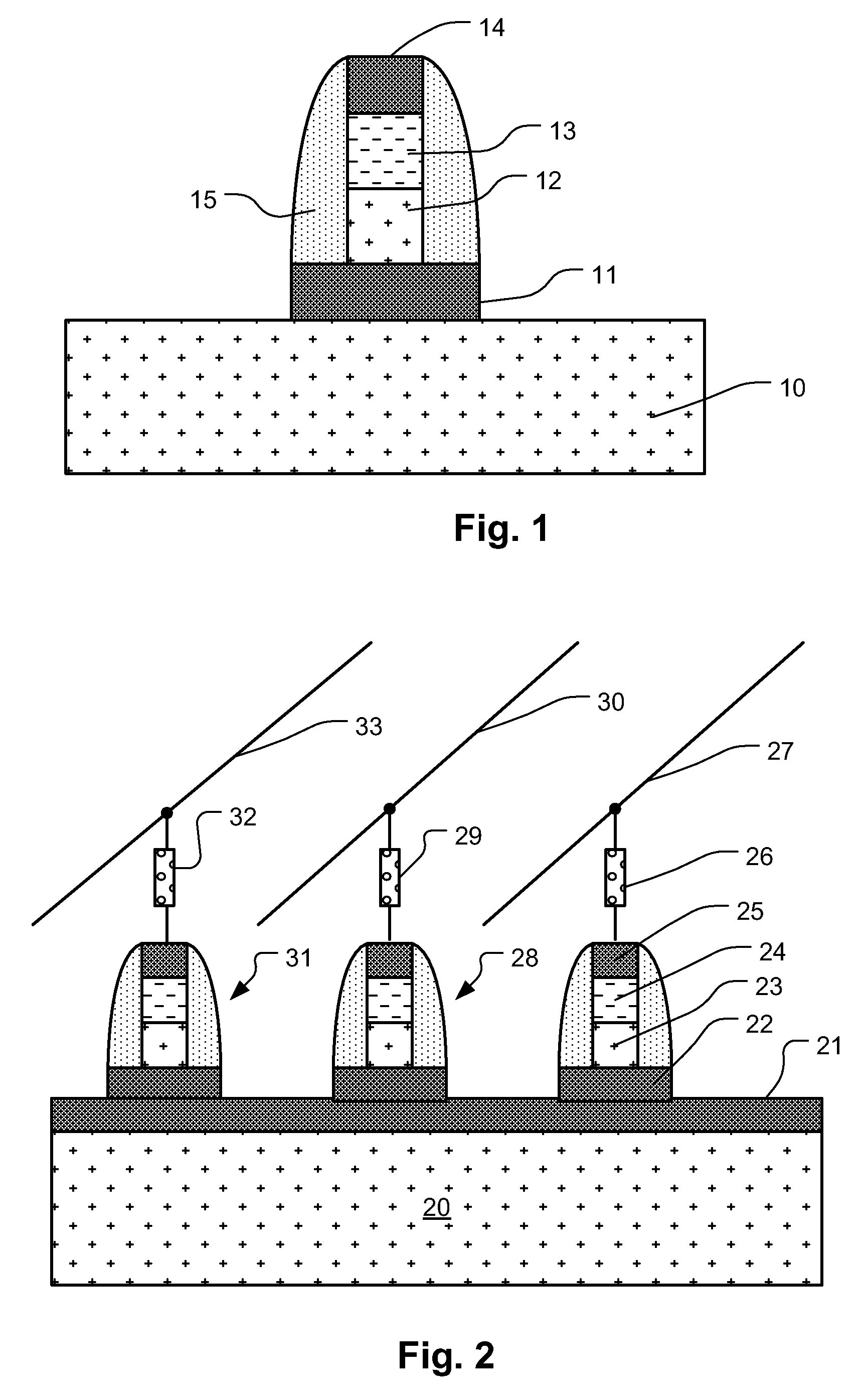
[0026]FIG. 1 illustrates an integrated circuit device formed on a single crystal silicon body 10, such as an epitaxial silicon layer in a silicon-on-insulator structure or a bulk silicon substrate. The device includes a silicide element 11, on top of which is a single crystal silicon node 12. A second semiconductor node 13 having a conductivity type opposite that of the single crystal silicon node 12 contacts the single crystal silicon node 12 forming a pn-junction therebetween. In the illustrated structure, a silicide cap 14 is formed on a second semiconductor node 13. Sidewall structures 15 isolate the pn-junction device from surrounding structures not shown. In the example of FIG. 1, a diode is shown using a single crystal silicon node 12 as one of the anode and cathode of the device. The single crystal silicon node 12 can be utilized in a variety of other structures as well, including transistors, and as a substrate on which additional layers can be formed which benefit from the...


PUM


Abstract

A silicide element separates a single crystal silicon node from an underlying silicon substrate, and is capable of acting as a conductive element for interconnecting devices on the device. The single crystal silicon node can act as one terminal of a diode, and a second semiconductor node on top of it can act as the other terminal of the diode. The single crystal silicon node can act as one of the terminals of the transistor, and second and third semiconductor nodes are formed in series on top of it, providing a vertical transistor structure, which can be configured as a field effect transistor or bipolar junction transistor. The silicide element can be formed by a process that consumes a base of a protruding single crystal element by silicide formation processes, while shielding upper portions of the protruding element from the silicide formation process.

Description

BACKGROUND[0001]1. Field of the Invention[0002]The present invention relates to integrated circuit devices including buried silicide conductors, and to methods for manufacturing such devices.[0003]2. Description of Related Art[0004]One common technology for interconnecting components on integrated circuits requires the use of buried diffusion lines, which consist of lines of implanted dopants in relatively high concentration, so that they act as conductors in the substrate. A problem that arises with the use of buried diffusion lines or other doped semiconductor features is the formation of parasitic devices. Semiconductor regions that are adjacent the buried diffusion lines can produce carriers during operation. These carriers can migrate into the buried diffusion lines, and activate parasitic devices causing breakdown or current leakage.[0005]Silicides are commonly used in integrated circuit manufacturing to increase the conductivity of doped silicon lines or elements. A common ve...

Claims


Application Information

Patent Timeline
IPC IPC(8): H01L29/78H01L21/44H01L23/48
CPCH01L21/743H01L27/1021H01L27/105H01L29/7827H01L29/861
Inventor LUNG, HSIANG-LANLAI, ERH-KUN
Owner MACRONIX INT CO LTD
Learn More