
Multiple-valued dram

a memory device and multi-value technology, applied in the field of memory devices with multiple values, can solve the problems of large amount of electric current consumed, defeat the advantages of mv sram, and reduce the number of devices used in the cell

Active Publication Date: 2010-06-24
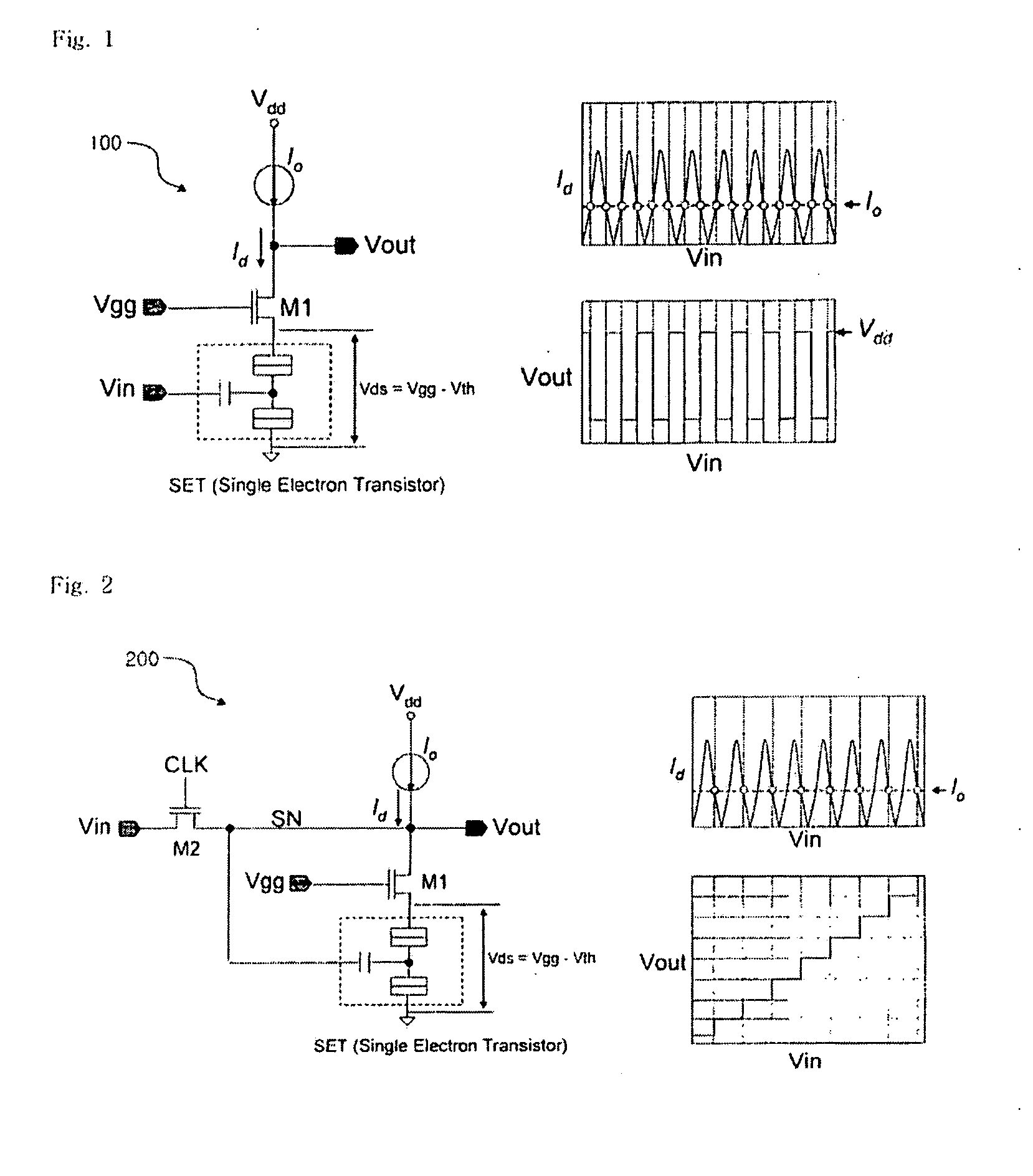
SONG BOK NAM +1
View PDF6 Cites 4 Cited by
  • Summary
  • Abstract
  • Description
  • Claims
  • Application Information

AI Technical Summary

Benefits of technology

[0024]The present invention is contrived to solve the above-mentioned problem. An advantage of the present invention is that it provides a multiple-valued (MV) DRAM device capable of storing multiple valued data other than binary data in a DRAM cell.
[0025]Another advantage of the present invention is that it provides an MV DRAM device applicable to a low-power application by eliminating a sense amplifier for a refresh operation using a Coulomb blockage characteristic of a single electron transistor (SET) device.
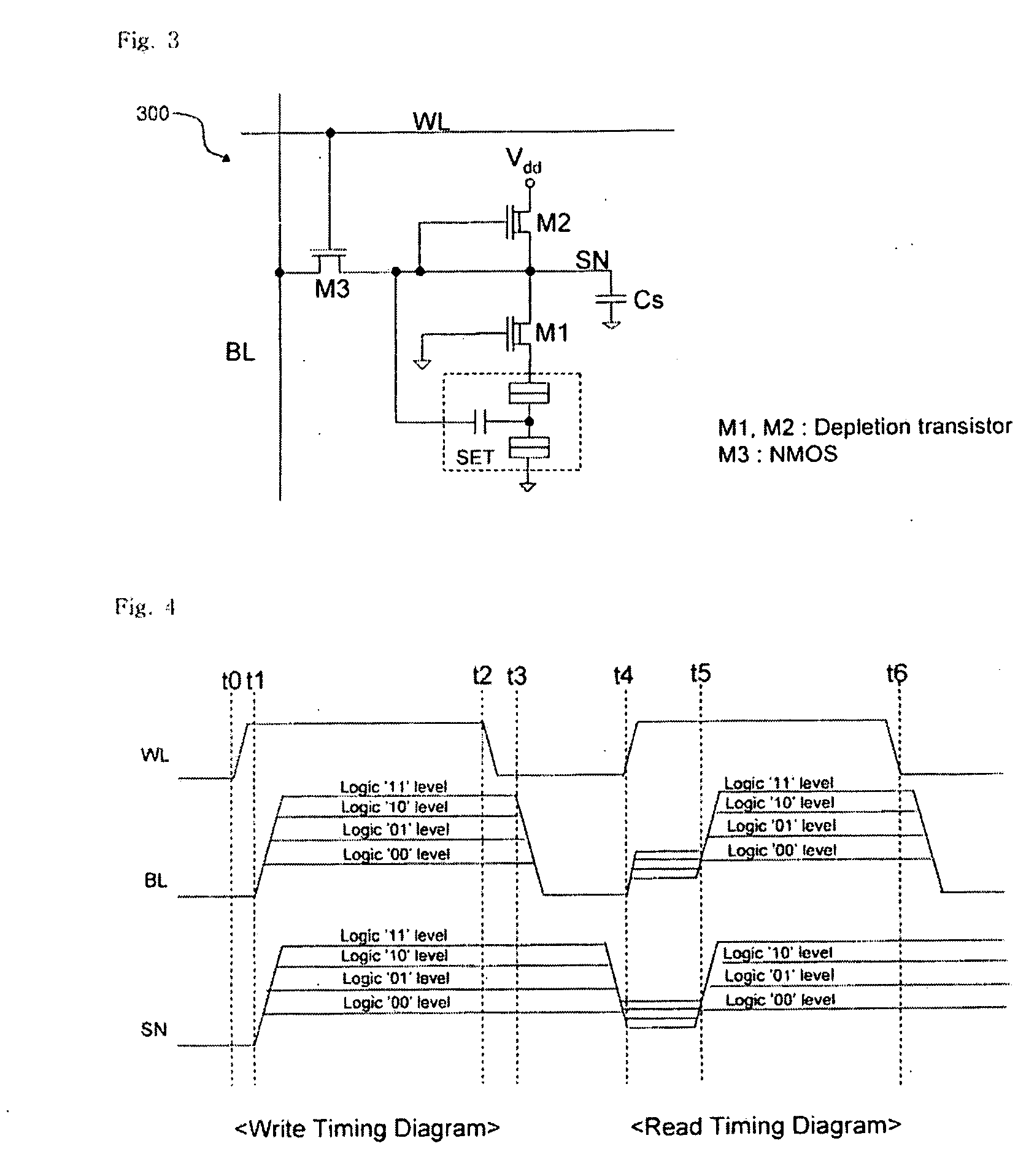
[0026]According to an aspect of the invention, there is provided an MV (multiple-valued) DRAM device for storing multiple value levels, the device including: one or more word lines; one or more bitlines; a DRAM cell connected to intersections of the word lines and the bitlines; a current source transistor having a source connected to a power supply voltage and a gate and a drain connected to the bitlines; an SET (single electron transistor) device having a gate connected to the bitlines and a source connected to the ground voltage; and a transistor connected between the bitlines and the drain of the SET device, wherein the gate of the transistor is connected to the ground voltage.
[0027]In the embodiments of the present invention, the DRAM cell may include a cell transistor having a gate connected to the word lines and a drain connected to the bitlines; and a cell capacitor connected between the source of the cell transistor and the ground voltage.
[0028]In the embodiments of the present invention, the SET device may include the source and the drain formed on a semiconductor substrate; a metal island disposed between the source and the drain so as to form a tunnel junction between the source and the drain; and the gate disposed in the vicinity of the metal island so as to control electric current flowing through the metal island.
[0029]In the embodiments of the present invention, the transistor connected between the bitlines and the drain of the SET device is a depletion transistor that maintains the drain voltage level of the SET device at the ground voltage, and the current source transistor is a depletion transistor.

Problems solved by technology

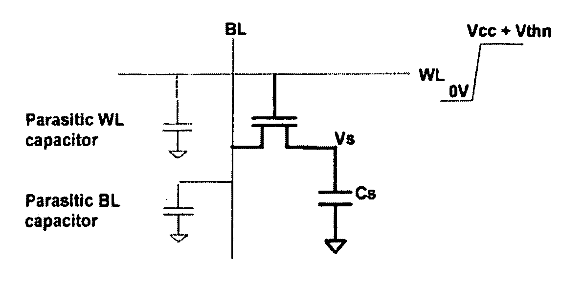
A multiple-valued memory is advantageous in that it increases storage density by increasing the number of bits stored in a cell but disadvantageous in that it decreases the number of device used in the cell, thereby defeating the advantages of the MV SRAM.
However, in the DRAM, a large amount of electric current is consumed in order to charge and discharge a relatively large parasitic capacitor of the bitline.
Since this consumed electric current increases a standby current, the DRAM is not suitable for a low-power application.

Method used


Image

  • Multiple-valued dram
  • Multiple-valued dram
  • Multiple-valued dram

Examples


Embodiment Construction

[0046]Hereinafter, exemplary embodiments of the present invention will be described in detail with reference to the attached drawings so that those skilled in the art can easily put the invention into practice. However, the invention may be embodied in a variety of forms, but is not limited to the exemplary embodiments. Like reference numerals in the drawings denote like elements.

[0047]FIG. 9 is a diagram showing an MV DRAM using an SET device according to an embodiment of the present invention.

[0048]Referring to FIG. 9, in an MV DRAM 800, a plurality of unit cells 810, 820, and 830 are arrayed at intersections of word lines WL and bitlines BL. The unit cells 810, 820, and 830 include one transistor M3 and one capacitor Cs similar to the DRAM. The bitline BL is connected to a current source transistor M2 for performing a refresh operation on the unit cells 810, 820, and 830. The bitline BL is also connected to an SET device and a first transistor M1.

[0049]The SET device includes a t...


PUM


Abstract

Provided herein is an MV DRAM device capable of storing multiple value levels using an SET device. The device includes one or more word lines; one or more bitlines; a DRAM cell connected to intersections of the word lines and the bitlines; a current source transistor having a source connected to a power supply voltage and a gate and a drain connected to the bitlines; an SET (single electron transistor) device having a gate connected to the bitlines and a source connected to the ground voltage; and a transistor connected between the bitlines and the drain of the SET device, wherein the gate of the transistor is connected to the ground voltage. According to the MV DRAM device of the present invention, since two or more multiple value data are stored in a cell, it is possible to increase the storage density of the device. In addition, since the MV DRAM device only needs to enable the word lines in order to rewrite the data, thereby requiring only a small amount of current flow, it is suitable for a low-power application.

Description

BACKGROUND[0001]1. Field of the Invention[0002]The present invention relates to a semiconductor memory apparatus and more particularly, to a multiple-valued (MV) dynamic random-access-memory (DRAM) device capable of storing multiple value levels using a single electron transistor (SET) device.[0003]2. Description of the Related Art[0004]Recently, a research has been conducted on an SET. The SET has advantages of increasing the integration degree of a circuit and decreasing power consumption. The SET also has inherent characteristics that the drain current of the SET increases and decreases periodically according to a gate bias. Researchers have made an effort to increase functionality of a circuit with fewer transistors by using such characteristics. In particular, the SET device has been proven to have characteristics highly suitable for applications in a multiple-valued logic circuit and therefore, incessant efforts have been made to use the SET device for the multiple-valued logi...

Claims


Application Information

Patent Timeline
Patent Type & Authority Applications(United States)
IPC IPC(8): G11C11/24G11C7/00
CPCG11C11/565G11C5/06G11C7/18G11C8/14G11C11/401G11C11/56
Inventor KYE, HUN WOOSONG, BOK-NAMCHOI, JUNG BUM
Owner SONG BOK NAM
Learn More