
Semiconductor device and method of manufacturing the same

a semiconductor and semiconductor technology, applied in the direction of semiconductor devices, semiconductor/solid-state device details, electrical equipment, etc., can solve problems such as product stress at a problematic level, bump crack or chip crack, etc., and achieve the effect of reducing stress and stress

Inactive Publication Date: 2010-05-20
RENESAS ELECTRONICS CORP
View PDF4 Cites 7 Cited by
  • Summary
  • Abstract
  • Description
  • Claims
  • Application Information

AI Technical Summary

Benefits of technology

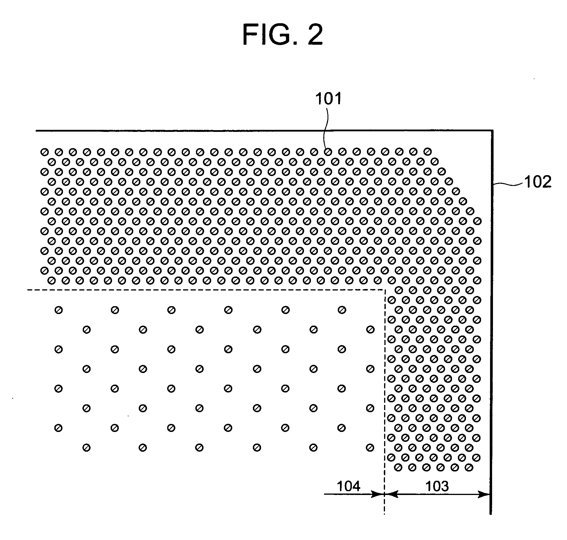
[0013]According to the present invention, stress occurring between the first region (9) and the second region (10) due to a difference in the density of the bumps is reduced by providing the third region (11). Thus, a bump crack and a chip crack due to the stress can be suppressed.
[0014]A semiconductor chip according to the present invention includes a bump formation surface (7) which faces a wiring board (1) when mounted on the wiring board (1) and which has a bump group (3) formed thereon, the bump group (3) electrically connected to the wiring board (1). In the semiconductor chip, the bump formation surface (7) includes: a first region (9) in which an area density of a region having bumps (3) arranged therein is a first density; a second region (10) in which an area density of a region having bumps (3) arranged therein is a second density lower than the first density; and a third region (11) for reducing stress occurring at the time of mounting the semiconductor chip on the wiring board (1). The third region (11) is provided in a border portion between the first region (9) and the second region (10). In the third region (11), an area density of a region having bumps (3) arranged therein is higher than the second density and is lower than the first density.
[0016]A method of manufacturing a semiconductor device according to the present invention includes the steps of: preparing a wiring board (1) including an electrode terminal group (5); preparing a semiconductor chip including a bump formation surface (7) which has a bump group (3) formed thereon, the bump formation surface (3) including a first region (9) in which an area density of a region having bumps (3) arranged therein is a first density, a second region (10) in which an area density of a region having bumps (3) arranged therein is a second density lower than the first density, and a third region (11) which is for reducing stress occurring at the time of mounting the semiconductor chip on the wiring board (1), which is provided in a border portion between the first region (9) and the second region (10), and in which an area density of a region having bumps (3) arranged therein is higher than the second density and is lower than the first density; and mounting the semiconductor chip on the wiring board (1) by heat treatment so that the bump group (3) faces the electrode terminal group (5).
[0017]The present invention provides a semiconductor device capable of reducing stress even when an arrangement of bumps has a density difference, and a method of manufacturing such a semiconductor device.

Problems solved by technology

Such stress may cause a bump crack or a chip crack.
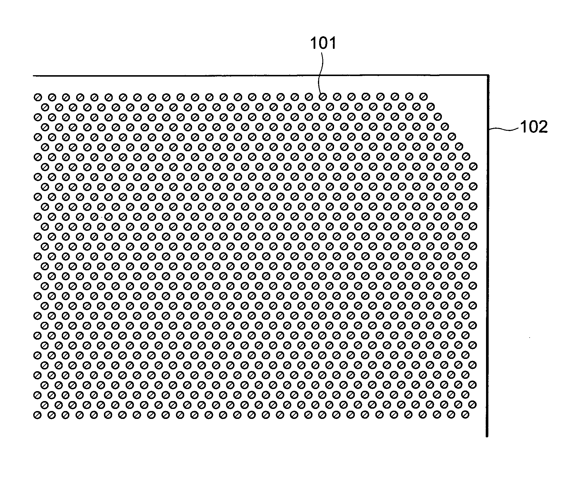
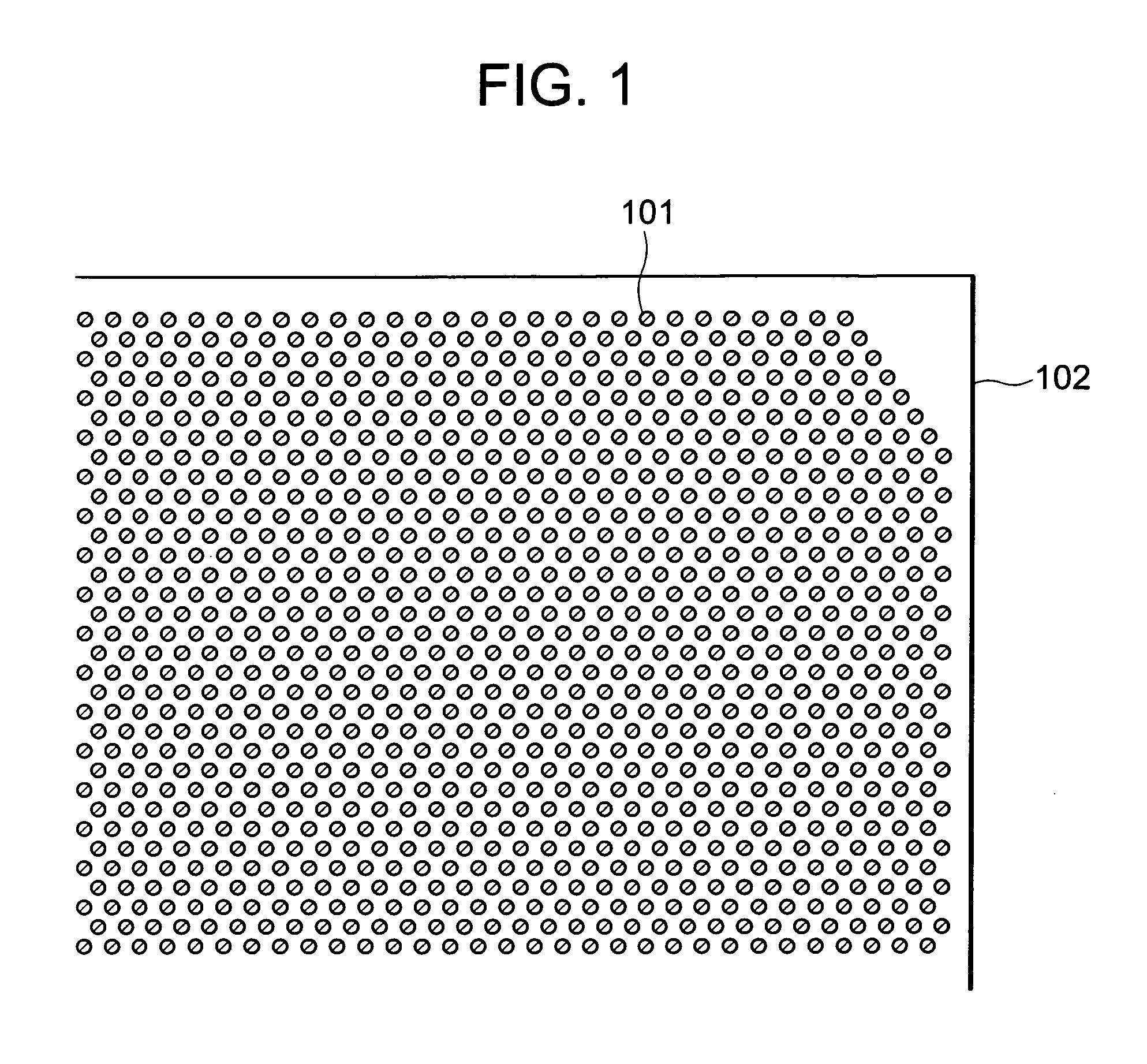
Apparently, there is a problem that stress at a problematic level for a product occurs when the arrangement of the bumps 101 has a notable density difference as shown in FIG. 3.

Method used


Image

  • Semiconductor device and method of manufacturing the same
  • Semiconductor device and method of manufacturing the same
  • Semiconductor device and method of manufacturing the same

Examples


first embodiment

[0028]A first embodiment according to the present invention will be described with reference to the drawings. FIG. 4 is a cross-sectional view showing a semiconductor device according to the present embodiment.

[0029]As shown in FIG. 4, the semiconductor device of the present embodiment includes a wiring board and a semiconductor chip 13. The wiring board 1 has a chip mounting surface 12. On the chip mounting surface 12, multiple electrode terminals 5 are formed as an electrode terminal group. Meanwhile, the semiconductor chip 13 includes a chip substrate 2 having a semiconductor integrated circuit formed thereon. The chip substrate 2 is provided with a bump formation surface 7. Multiple bumps 3 are formed on the bump formation surface 7 as a bump 3 group. The semiconductor chip 13 is mounted on the wiring board 1 so that the bump formation surface 7 would face the chip mounting surface 12. An arrangement pattern of the bumps 3 on the bump formation surface 7 is the same as an arrang...

second embodiment

[0043]Next, a second embodiment will be described. FIG. 8 shows a bump formation surface 7 of a semiconductor device according to the second embodiment. In the present embodiment, the size and the arrangement of bumps 3 in a third region 11 are different from those in the first embodiment. The other points may be the same as the first embodiment, and thus the detailed description thereof is omitted here.

[0044]In the present embodiment, as in the case of the first embodiment, the region of the third region 11 having the bumps 3 arranged thereon has an area density (third density) which is higher than a second density and is lower than a first density. However, in the present embodiment, the number of the bumps 3 arranged per unit area in the third region 11 is the same as that in the second region 10. Meanwhile, the size of each of the bumps 3 arranged in the third region 11 is larger than the size of each of the bumps 3 arranged in the first region 9 and the second region 10. Note t...

third embodiment

[0049]Next, a third embodiment of the present invention will be described. FIG. 10 shows a bump formation surface 7 of a semiconductor device according to the third embodiment. In the present embodiment, a bump group provided on the bump formation surface 7 includes actual bumps 3-1 and dummy bumps 3-2. The other points maybe the same as the above-described embodiments, and thus the detailed description thereof is omitted here.

[0050]The actual bumps 3-1 are bumps used for electrical connection between a semiconductor chip 13 and a wiring board 1. On the other hand, the dummy bumps 3-2 are provided to control the area density of a region where the bumps are arranged, and are not used for the electrical connection between the semiconductor chip 13 and the wiring board 1.

[0051]According to the present embodiment, the stress can be reduced by the same effects as the above-described embodiments. In addition, the area density of a region where the bumps 3 are arranged can be controlled by...


PUM


Abstract

Provided are a semiconductor device capable of reducing stress due to a density difference in the arrangement of bumps, and a method of manufacturing the semiconductor device. The semiconductor device includes: a wiring board including an electrode terminal group; a semiconductor chip including a bump formation surface where a bump group is formed and being mounted on the wiring board by using the bump group. The bump formation surface includes a first region where an area density of a region having bumps arranged therein is a first density, a second region where an area density of a region having bumps arranged therein is a second density lower than the first density, and a third region provided in a border portion between the first and second regions. In the third region, an area density of a region having bumps arranged therein is above the second density and below the first density.

Description

BACKGROUND OF THE INVENTION[0001]1. Field of the Invention[0002]The present invention relates to a semiconductor device and a method of manufacturing the semiconductor device.[0003]2. Description of the Related Art[0004]A semiconductor package (a semiconductor device) includes a semiconductor chip and a wiring board on which the semiconductor chip is mounted. The semiconductor chip is provided with a bump formation surface on which protruding bumps are formed. Solder, for example, is used as a material for the bumps. The semiconductor chip is mounted on the wiring board by using the bump formation surface.[0005]In such a semiconductor device, stress is applied to the semiconductor chip and the bumps at the time of mounting the semiconductor chip or after the mounting in some cases. For example, in a case where flux is used to form the bumps, the semiconductor chip is mounted on the wiring substrate by a heat treatment such as an IR reflow treatment. In this mounting, stress sometime...

Claims


Application Information

Patent Timeline
IPC IPC(8): H01L23/498H01L21/768
CPCH01L23/49838H01L24/17H01L2224/0401H01L2224/0603H01L2224/13099H01L23/49811H01L2924/01077H01L2924/14H01L24/13H01L2924/01006H01L2924/01033H01L2224/1403H01L2224/14
Inventor TAKEDA, KUNIHIRO
Owner RENESAS ELECTRONICS CORP
Learn More