
High Resolution Imaging System

a high-resolution, imaging system technology, applied in the field of radiographic imaging, can solve the problem of not using a scanning system coupled to the disclosed position sensitive digital detection method

Inactive Publication Date: 2010-05-13
NOVA R&D
View PDF17 Cites 39 Cited by
  • Summary
  • Abstract
  • Description
  • Claims
  • Application Information

AI Technical Summary

Benefits of technology

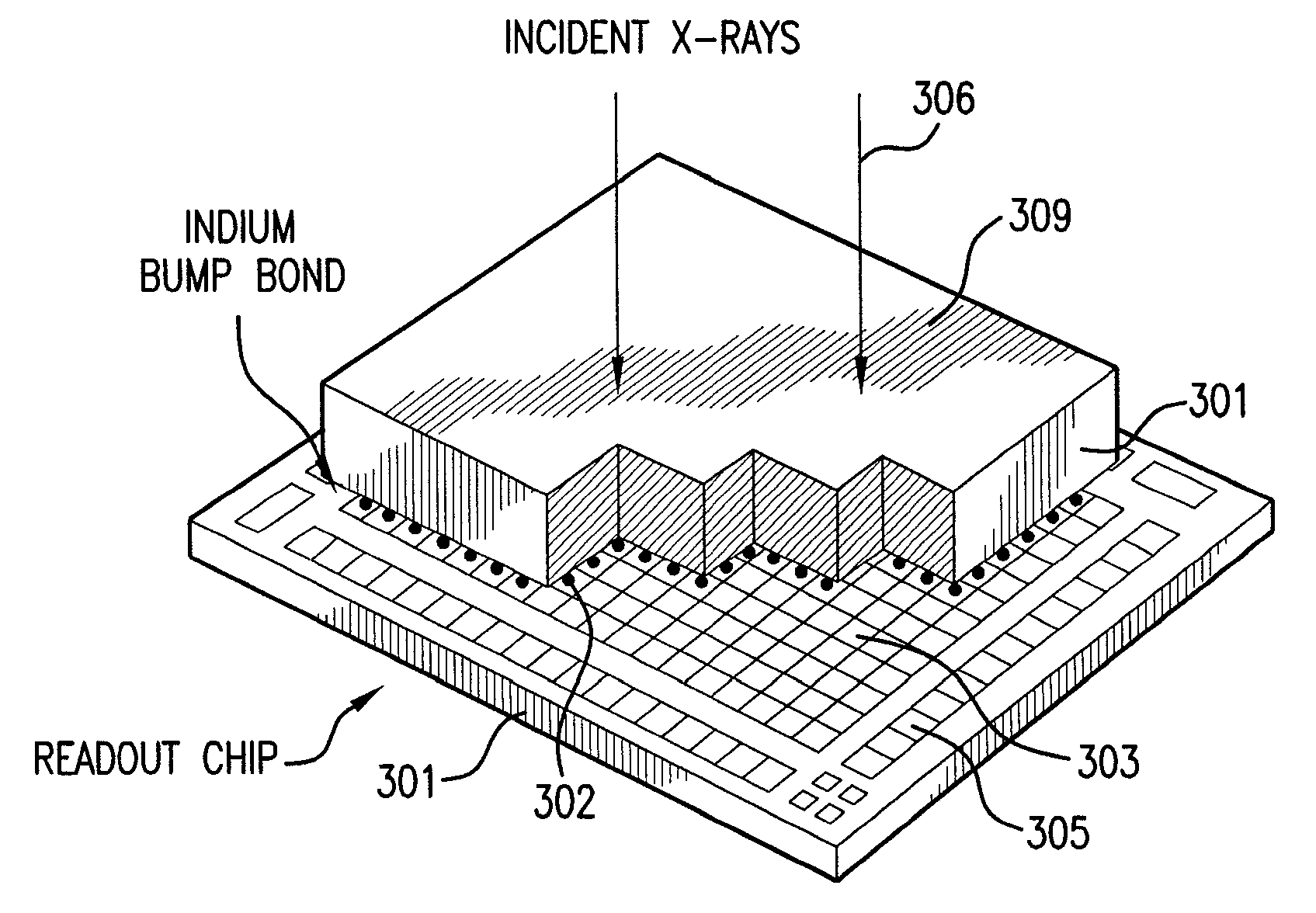
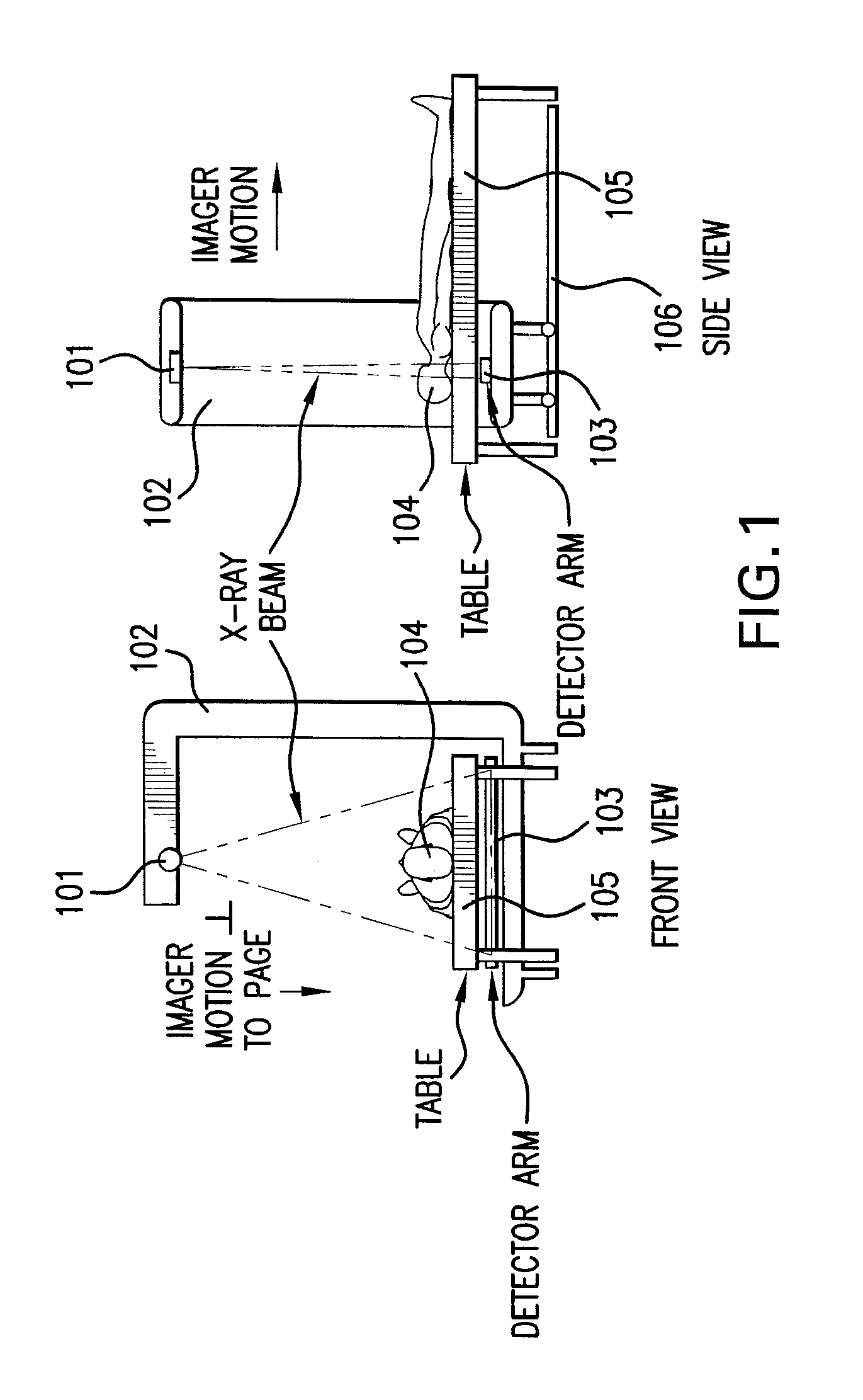
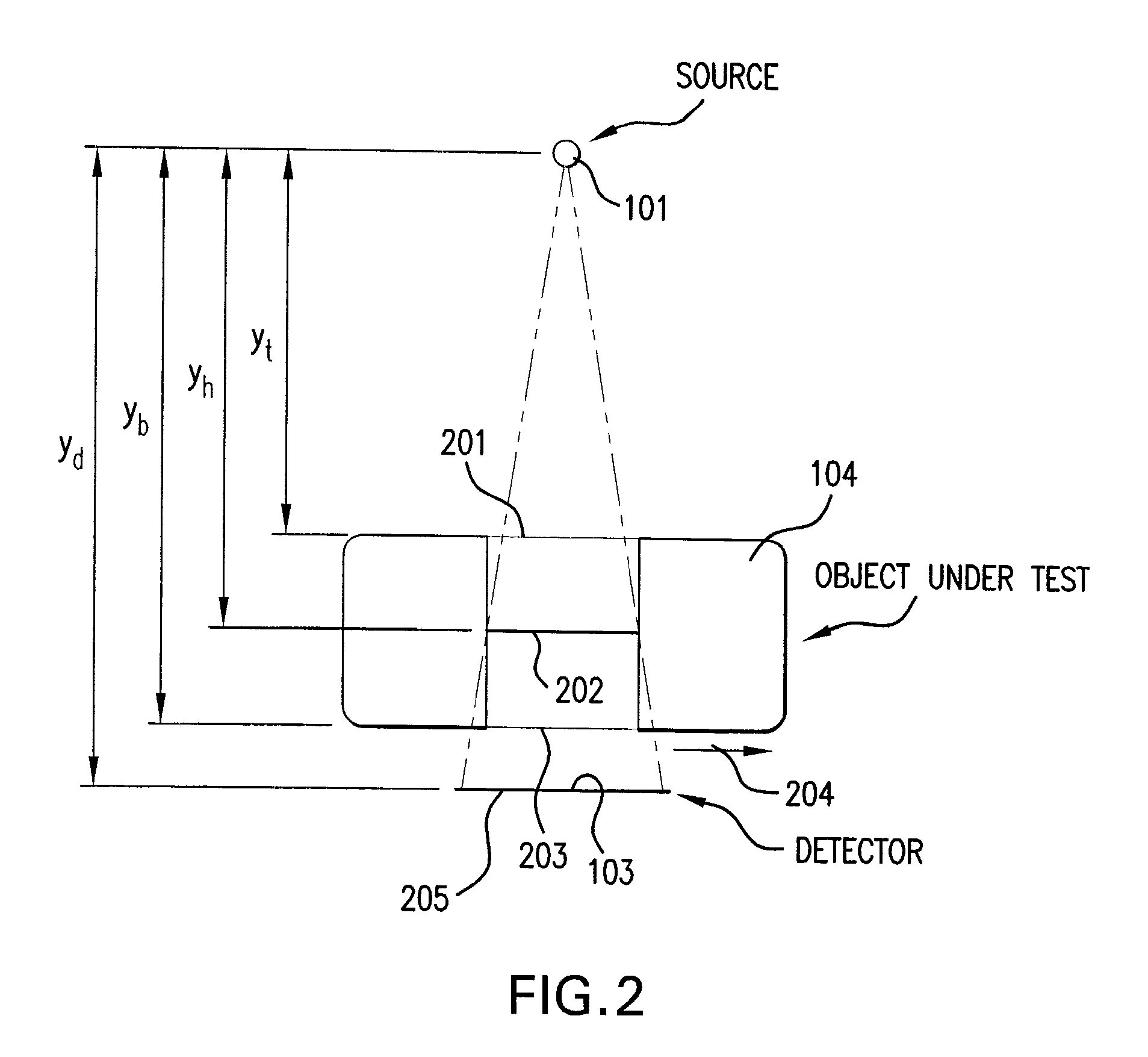
[0008]The disclosed fast full body digital radiography system is a direct imaging digital radiography system and will not use radiographic film. The solid state pixel detectors have high MTF, about 5 to 8 line pairs per mm, approaching the resolution of a screen-film system. The system has high DQE, about 50%-70%, and high contrast, therefore low dose to the patient. The linear array has a low projected area for x-rays scattered in the patient's body and therefore low background and higher signal to noise ratio. The images are taken in scanning mode using the Time Delayed Integration (TDI) technique. This technique produces uniform images without flawed or dead image pixels even if there are a moderate number of random defective detector pixels.
[0009]This is a low cost, digital (no film), high resolution, low dose and fast general whole or partial body radiography system that will allow immediate and fast prescreening of patients arriving at emergency rooms (ER). In human diagnostic applications the system is capable of screening a whole body or parts of a body in several seconds and displaying the image in real time on a high resolution computer screen without the need for accurate patient positioning and elaborate exposure setting. Small and portable machines can be used in ambulances, special imaging vans, rural and remote communities, during catastrophic events, on battlefields and in field hospitals.

Problems solved by technology

However, use of a scanning system coupled to the disclosed position sensitive digital detection methods are not.

Method used


Image

  • High Resolution Imaging System
  • High Resolution Imaging System
  • High Resolution Imaging System

Examples


first embodiment

[0110]The first embodiment is to use a passive resistance in the feedback circuit. This is limited on how much resistance can be built into the chip at the feedback loop of the input amplifier at the input of each channel.

second embodiment

[0111]The second embodiment is to use resistive multiplier feedback circuit, which is an innovative way to create a linear element (a resistor) with active MOSFET components. This circuit uses current mirror divider circuits configured as an extremely small transconductance amplifier to make an equivalent resistor greater than 200 MOhm (2×10+8 Ohms). A small 100 KOhm resistor is used as the reference device for this circuit. A measurement of current going through the 100 KOhm resistor is made and a new current level of 1 / 200th the magnitude is driven at the output pin. The resistive multiplier circuit achieves high resistances in a small area because it replaces the large area required for a large linear resistor (>108 Ohms) with a circuit of area 0.042 mm2. A resistor of 200 MOhm made from 1 kOhm / square (Ohms cm length / width thickness) polysilicon would be 1 mm2 in size for a 0.5 μm process. Also, a large resistor element would suffer from RC delay effects, which the active circuit...

third embodiment

[0112]The third embodiment is to use a MOSFET transistor as a resistive feedback circuit with its resistance is externally controlled. Such circuitry can be used to produce a large resistance feedback component, >109 Ohms. It has a much smaller area, about 0.001 mm2. Therefore, it is especially appropriate to use for smaller pixel sizes such as 250×250 μm2 pixel pitch. It can be added as an option to the resistive multiplier circuit during the prototype fabrication so that it can be tested and evaluated in comparison to the resistive multiplier circuit. Unfortunately, MOSFET resistive element is nonlinear and also it may not be used with the pole-zero cancellation circuit.


PUM

PropertyMeasurementUnit
sizeaaaaaaaaaa
sizesaaaaaaaaaa
lengthaaaaaaaaaa

Abstract

New sensors, pixel detectors and different embodiments of multi-channel integrated circuit are disclosed. The new high energy and spatial resolution sensors use solid state detectors. Each channel or pixel of the readout chip employs low noise preamplifier at its input followed by other circuitry. The different embodiments of the sensors, detectors and the integrated circuit are designed to produce high energy and / or spatial resolution two-dimensional and three-dimensional imaging for different applications. Some of these applications may require fast data acquisition, some others may need ultra high energy resolution, and a separate portion may require very high contrast. The embodiments described herein addresses these issues and also other issues that may be useful in two and three dimensional medical and industrial imaging. The applications of the new sensors, detectors and integrated circuits addresses a broad range of applications such as medical and industrial imaging, NDE and NDI, security, baggage scanning, astrophysics, nuclear physics and medicine.

Description

CROSS-REFERENCE TO RELATED APPLICATION[0001]This application is a divisional of U.S. patent application Ser. No. 11 / 090,123, filed on Mar. 28, 2005. U.S. patent application Ser. No. 11 / 090,123 claims the benefit of U.S. Provisional Application Ser. No. 60 / 556,507 filed on Mar. 26, 2004, entitled HIGH RESOLUTION IMAGING SYSTEM. The afore-mentioned application is hereby incorporated by reference herein in its entirety, including but not limited to those portions that specifically appear hereinafter, the incorporation by reference being made with the following exception: In the event that any portion of the above-referenced application is inconsistent with this application, this application supercedes said above-referenced applications.STATEMENT REGARDING FEDERALLY SPONSORED RESEARCH OR DEVELOPMENT[0002]Some parts of the invention were made with U.S. Government support under Contract Numbers DAAE 30-02-C-1015, DAAE 30-03-C-1074, and DAMD 17-01-1-0356, which are awarded by the Departmen...

Claims


Application Information

Patent Timeline
Patent Type & Authority Applications(United States)
IPC IPC(8): G01T1/24H01L21/50H05K3/30H01L31/02
CPCG01T1/247G01T1/249Y10T29/49126H01L2224/16145H01L2224/4847
Inventor TUMER, TUMAYCLAJUS, MARTIN
Owner NOVA R&D
Learn More