
Memory controller, nonvolatile memory device, access device, and nonvolatile memory system

a memory controller and non-volatile memory technology, applied in the field of memory controllers, non-volatile memory devices, access devices, and non-volatile memory systems, can solve the problem of requiring a relatively long time to wri

Active Publication Date: 2010-05-06
PANASONIC CORP
View PDF9 Cites 31 Cited by
  • Summary
  • Abstract
  • Description
  • Claims
  • Application Information

AI Technical Summary

Benefits of technology

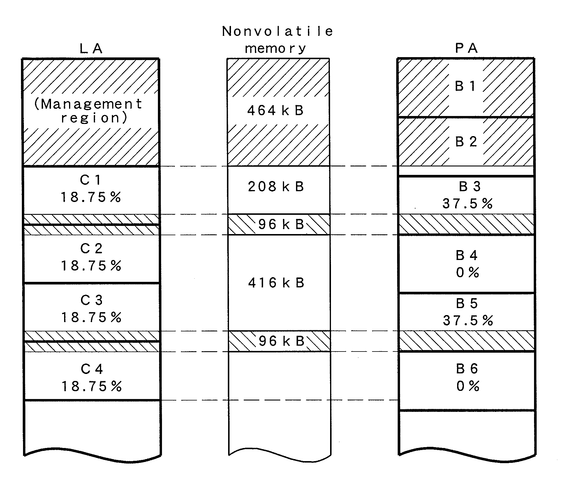
[0050]According to the present invention, when an access device designates a transfer rate required to a nonvolatile memory device, a remaining capacity corresponding to a transfer rate designated by an access device can be obtained on the basis of a data recording state for each block on a physical address space of a nonvolatile memory. The access device accordingly can obtain a correct remaining capacity of the nonvolatile memory device corresponding to the transfer rate requested by an application of the access device and information, for example, a remaining recording time or remaining recording number which can be calculated from the remaining capacity.

Problems solved by technology

The flash memory incorporated in products, for example, the semiconductor memory card and a portable audio apparatus requires relatively long time to write and read data to and from a memory cell array, a storage unit.

Method used


Image

  • Memory controller, nonvolatile memory device, access device, and nonvolatile memory system
  • Memory controller, nonvolatile memory device, access device, and nonvolatile memory system
  • Memory controller, nonvolatile memory device, access device, and nonvolatile memory system

Examples


Embodiment Construction

[0088]In the present embodiment, an access device designates a file ID and a nonvolatile memory device maps file data related to the file ID on the physical address space of a nonvolatile memory without relating different address spaces of the access device and the nonvolatile memory device with each other. The inventors found that the problems caused when a state of the physical address space is related to a state of the logical address space can be solved by this method. The method is hereinafter referred to as a file level access method.

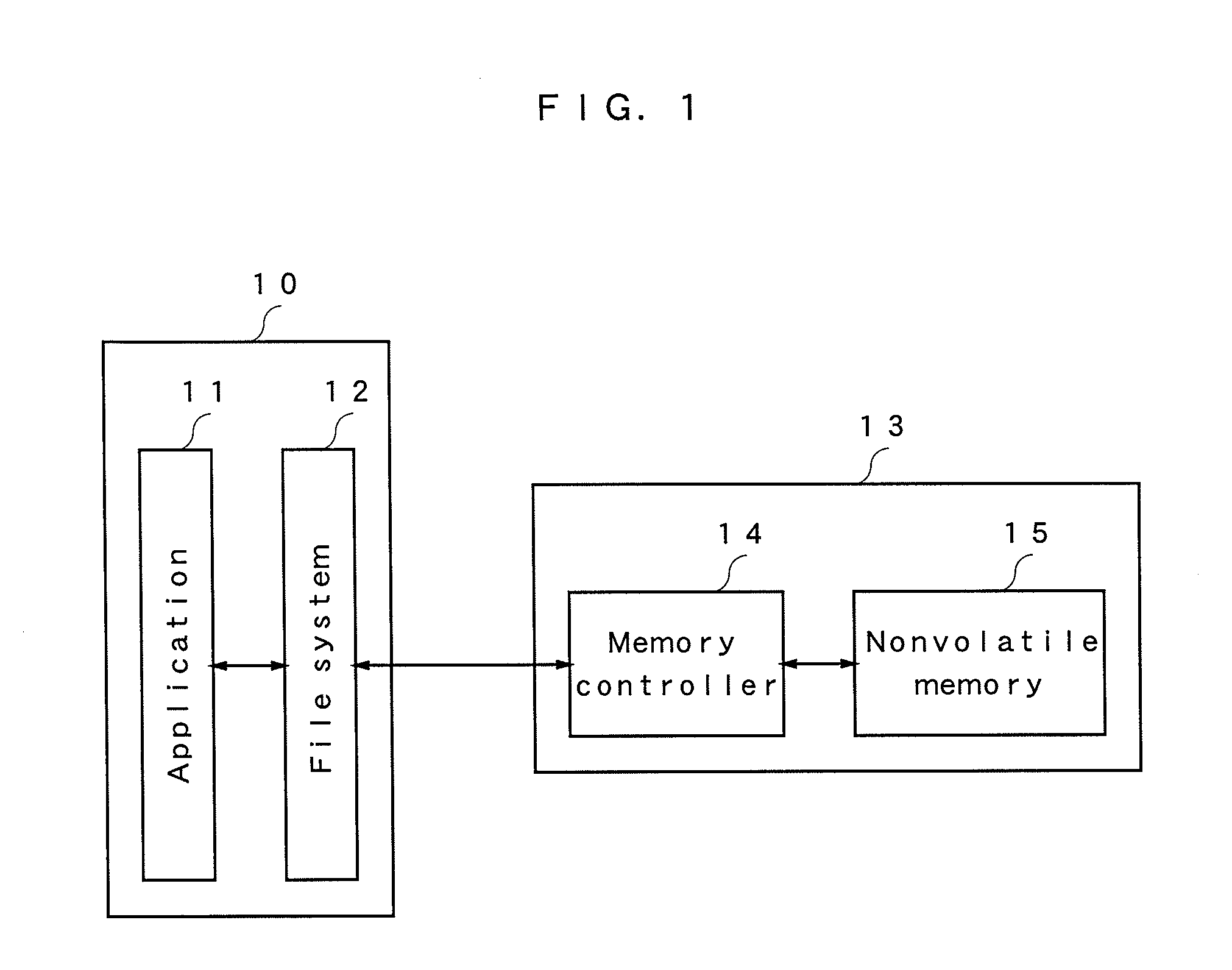
[0089]Referring to FIG. 9 to FIG. 16B, an embodiment of a nonvolatile memory system according to the present invention will be explained. FIG. 9A is a block diagram showing an access device 100 of the nonvolatile memory system in the present embodiment, and FIG. 9B shows a non volatile memory device 200.

[0090]The nonvolatile memory system includes the access device 100 and the nonvolatile memory device 200, and the access device 100 includes a use...


PUM


Abstract

Without corresponding to different address spaces between an access device (100) and a nonvolatile memory device (200), the access device (100) designates a file ID to manage a data storing state only in a physical address space in the nonvolatile memory device (200). The access device (100) sends the nonvolatile memory device (200) a transfer rate through a transfer rate transmitting unit (121). A filling-up rate calculating unit (251) calculates a filling-up rate of a physical block corresponding to an assurance speed required by the access device (100). A remaining amount corresponding to the transfer rate is sought by using the calculated rate and is transmitted to a remaining amount receiving unit (122) of the access device (100).

Description

TECHNICAL FIELD[0001]The present invention relates to a nonvolatile memory device such as a semiconductor memory card having a nonvolatile memory, a memory controller for controlling this device, an access device for accessing said nonvolatile memory device, and a nonvolatile memory system configured by adding the access device as a component to said nonvolatile memory device.BACKGROUND ART[0002]A nonvolatile memory device having a rewritable nonvolatile memory is increasingly demanded mainly for a semiconductor memory card. The semiconductor memory card is high-price compared to an optical disk, media of tape, and the like, however, the demand as a recording medium is widely increasing for a portable apparatus such as a digital still camera and a mobile phone because of merits such as small-size, lightweight, vibration resistance, and easy handling. This semiconductor memory card has a flash memory as a nonvolatile main memory and has a memory controller for controlling the memory....

Claims


Application Information

Patent Timeline
Patent Type & Authority Applications(United States)
IPC IPC(8): G06F12/00G06F12/02
CPCG06F12/0246G06F2212/7201G06F2212/7202
Inventor ONO, TADASHIADACHI, TATSUYANAKANISHI, MASAHIROMAEDA, TAKUJI
Owner PANASONIC CORP
Learn More