Organic dry jet printing head, and printing device and method using the same

Inactive Publication Date: 2010-04-22
KOREA ADVANCED INST OF SCI & TECH
View PDF5 Cites 16 Cited by
  • Summary
  • Abstract
  • Description
  • Claims
  • Application Information

AI Technical Summary

Benefits of technology

[0019]Accordingly, the present invention has been made to solve the above-mentioned problems, and an object of the present invention is to provide an organic dry jet printing head and a printing device and method using the same, in which processes can be performed at atmospheric pressure, a large-area organic electronic device can be manufactured and high-resolution patterns can be printed, thereby improving productivity and economic efficiency.
[0020]Another object of the present invention is to provide an organic dry jet printing head and a printing device and method using the same, in which a pattern (thin film) can be formed through the repetitive injection of a high-speed jet by regularly and repeatedly opening and closing an on-off valve in a pattern (thin film) forming region using the on-off valve and a control unit, so that the spreading of the pattern is minimized even at atmospheric pressure, thereby forming a uniform and precise pattern.
[0027]Further, the on-off valve may be a microelectromechanical system (MEMS) shutter which can finely control the nozzle.

Problems solved by technology

First, since high vacuum is required, equipment costs are increased and maintenance becomes difficult.
Second, since a large part of expensive semiconductor materials which are sublimed into gas is adhered to the inner wall of the vacuum chamber, it is discarded without being used to fabricate an organic electronic device, so that the loss of the expensive semiconductor materials is increased.
Third, there is a restriction in fabrication of large-area organic electronic devices due to limitation in the size of the vacuum chamber and drooping of a shadow mask, and it is difficult to realize high-resolution patterns.
For these reasons, the thermal evaporation-vacuum sublimation process using the ultra-high vacuum chamber is problematic in that it is difficult to realize high-resolution patterns required to design an organic electronic device, and it is difficult to fabricate a large-area organic electronic device, so that the production of the organic electronic device per hour is remarkably decreased, with the result that the production time of the organic electronic device is increased and the price thereof also is inevitably increased.
However, this OVPD is also problematic in that it cannot overcome the above problems because it is not a printing type deposition process and thus needs a shadow mask.
However, the solution process using an ink jet printing or stamping process is also problematic in that the organic electronic devices manufactured using this solution process have much lower efficiency and lifespan than the organic electronic devices manufactured using the thermal evaporation-sublimation process, and in that it is difficult to obtain an organic semiconductor thin film having uniform thickness due to the non-uniformity of film resulting from such as the coffee-stain effect which occurs in the solution process.
However, the ink jet printing process or the stamping process is problematic in that it is difficult to manufacture the organic electronic device having the multi-layer thin film structure.
Of these two processes, the former is problematic in that an apparatus for generating a guard flow is additionally required and a large amount of gas is consumed although it can be used at atmospheric pressure, and the latter is problematic in that high-resolution patterns can be formed only when an organic material is deposited on a substrate in a vacuum of about 10 Torr or less, which is lower than an atmospheric pressure of 760 Torr.
Most of all, this organic vapor jet printing (OVJP) process is problematic in that the thickness of an organic film can be non-uniform (for example, the thickness of the organic film is thicker at the corners thereof) depending on its patterns because the deposition of the organic material is conducted using a continuous gas flow, and in that it becomes sensitive to the atmospheric environment because the gas must flow at a low flow velocity in order to minutely adjust the thickness of the organic film.
No. 2005-0087131 filed by M. Shtein, the technology disclosed in Korean Unexamined Patent Application Publication No. 10-2004-44534 is problematic in that it is difficult to adjust the thickness of an organic film (pattern) because the organic film (pattern) is formed by continuous gas flow, and in that the pattern circumferentially spreads at atmospheric pressure because the gas must flow at a low flow velocity in order to minutely adjust the thickness of the organic film.

Method used


Image

  • Organic dry jet printing head, and printing device and method using the same
  • Organic dry jet printing head, and printing device and method using the same
  • Organic dry jet printing head, and printing device and method using the same

Examples


Embodiment Construction

[0050]Hereinafter, preferred embodiments of the present invention will be described in detail with reference to the attached drawings.

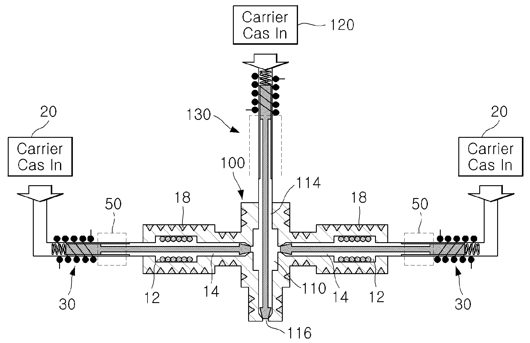
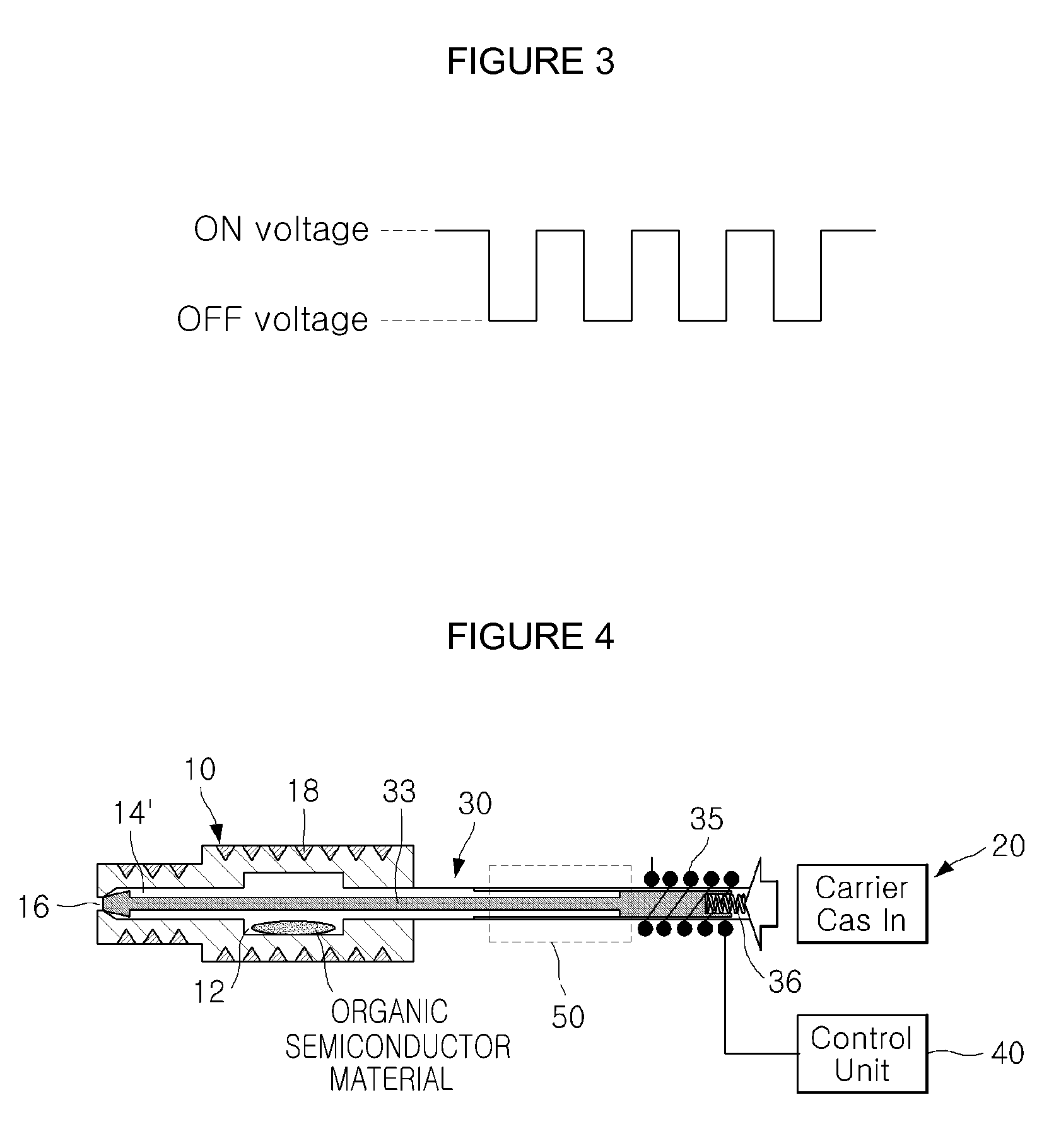
[0051]FIG. 2 is a sectional view showing an organic dry jet printing head according to an embodiment of the present invention, and FIG. 3 is a view showing an example of control signal settings in an organic dry jet printing head according to an embodiment of the present invention.

[0052]An organic dry jet printing head according to an embodiment of the present invention includes a head body 10 storing a pattern forming material such as an organic semiconductor material (hereinafter, referred to as “organic material”) for forming an organic semiconductor thin film or fine pattern (hereinafter, commonly referred to as “thin film”) on a substrate. The head body 10 is provided therein with an organic material storage chamber 12 for storing the organic material and a carrier gas passage 14 passing through the head body 10 via the organic material storage c...


PUM

PropertyMeasurementUnit
Temperatureaaaaaaaaaa
Thicknessaaaaaaaaaa
Pressureaaaaaaaaaa

Abstract

Disclosed herein is an organic dry jet printing head and a printing device and method using the same, in which a pattern (thin film) can be formed through the repetitive injection of a high-speed jet by regularly and repeatedly opening and closing an on-off valve in a pattern (thin film) forming region using the on-off valve and a control unit. The organic dry jet printing head and the printing device and method using the same are advantageous in that processes can be performed at atmospheric pressure, a large-area organic electronic device can be manufactured and high-resolution patterns can be printed, thereby improving productivity and economic efficiency.

Description

CROSS-REFERENCES TO RELATED APPLICATION[0001]This patent application claims the benefit of priority under 35 U.S.C. § 119 from Korean Patent Application No. 10-2008-0103751 filed on Oct. 22, 2008, the contents of which are incorporated herein by reference.BACKGROUND OF THE INVENTION[0002]1. Field of the Invention[0003]The present invention relates to a printing device and method for forming an organic semiconductor thin film at the time of fabrication of organic electronic devices, such as organic light emitting displays (OLEDs), organic solar cells (organic photovoltaic cells (OPVs)), organic thin film transistors (OTFTs) and the like.[0004]2. Description of the Related Art[0005]Organic electronic devices are being greatly spotlighted in the next-generation electronics industries. Among them, OLEDs are believed to be core parts of next-generation flat panel displays and flexible displays, OPVs have lately been researched actively according to the importance of the energy industry, ...

Claims


Application Information

Patent Timeline
IPC IPC(8): B41J29/38B05D5/12
CPCB41J2/005B41J2202/09C23C14/04H01L51/0005C23C14/228C23C14/243C23C14/12H10K71/135B41J2/235C23C16/00B41J3/00
Inventor YOO, SEUNGHYUPYUN, CHANGHUNCHO, HYUNSU
Owner KOREA ADVANCED INST OF SCI & TECH
Why Eureka
Try Eureka