Sheet-like composite electronic component and method for manufacturing same

Inactive Publication Date: 2010-04-15
PANASONIC CORP
View PDF0 Cites 86 Cited by
  • Summary
  • Abstract
  • Description
  • Claims
  • Application Information

AI Technical Summary

Benefits of technology

[0010]According to this configuration, by laminating electronic components made of a plurality of thin film electronic components, a sheet-like composite electronic component can be formed, so that, as compared to a configuration that electronic components are arranged on a flat surface, reduction of a size is more available. Further, since the thin film electronic components are very thin as compared to the chip components that are generally used, even if they are laminated, the thickness thereof can be made thinner than that of the chip component or the like. Therefore, reduction of a thickness is possible in addition to reduction of a size.
[0012]According to this method, since the first thin film electronic component and the second thin film electronic component are divided into the first resin sheet and the second resin sheet to be formed, respectively, each step can be simplified. Further, the adhering and the interlayer electric connection are carried out collectively, and then, the first resin sheet and the second resin sheet are cut to manufacture a composite electronic component, so that it is possible to prevent a defect on manufacturing and the composite electronic component can be manufactured with a good yield rate.

Problems solved by technology

However, in mere reduction of a size and mere reduction of a thickness of the chip component, it is expected that there is a very difficulty in a manufacturing step such as mounting of the chip components on a circuit substrate or the like.
However, this composite electronic component is composed in such a manner that the electronic components formed by a thin film are aligned on a flat surface and in such an arrangement configuration on a flat surface, there is a limitation in an integration degree of the electronic component.
In addition, the case that the previously manufactured thin film electronic component becomes a defective good due to an influence of a manufacturing step of the thin film electronic component to be laminated on this is easily generated.
As a result, a yield rate as a laminated finished component-incorporated flexible circuit substrate is made low, so that there is a problem that this becomes a high price.

Method used


Image

  • Sheet-like composite electronic component and method for manufacturing same
  • Sheet-like composite electronic component and method for manufacturing same
  • Sheet-like composite electronic component and method for manufacturing same

Examples


first exemplary embodiment

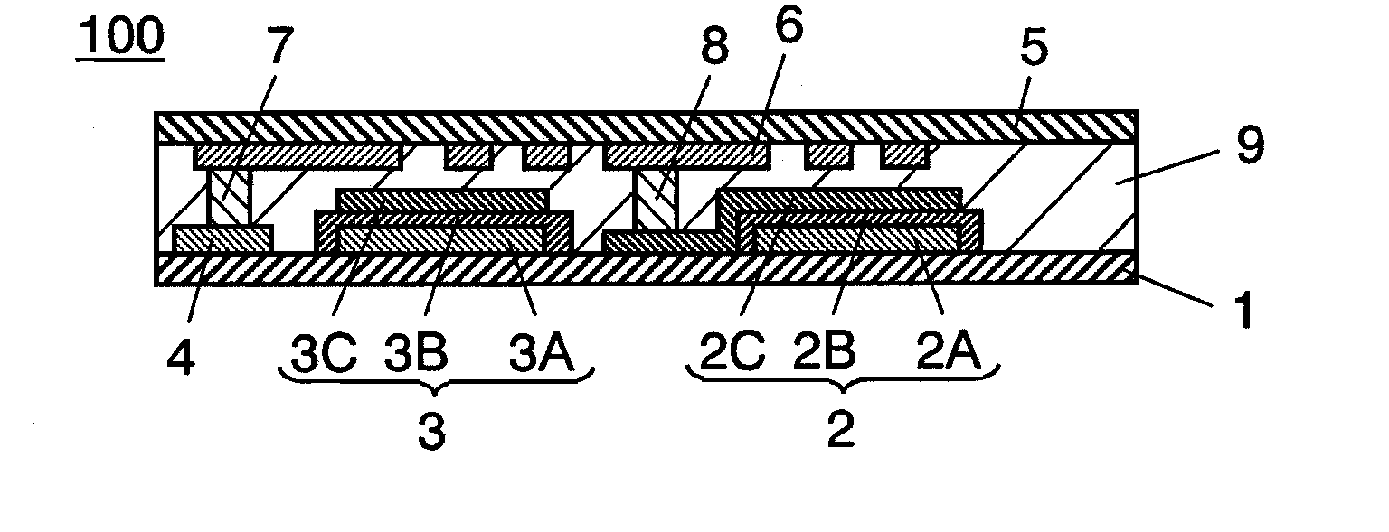
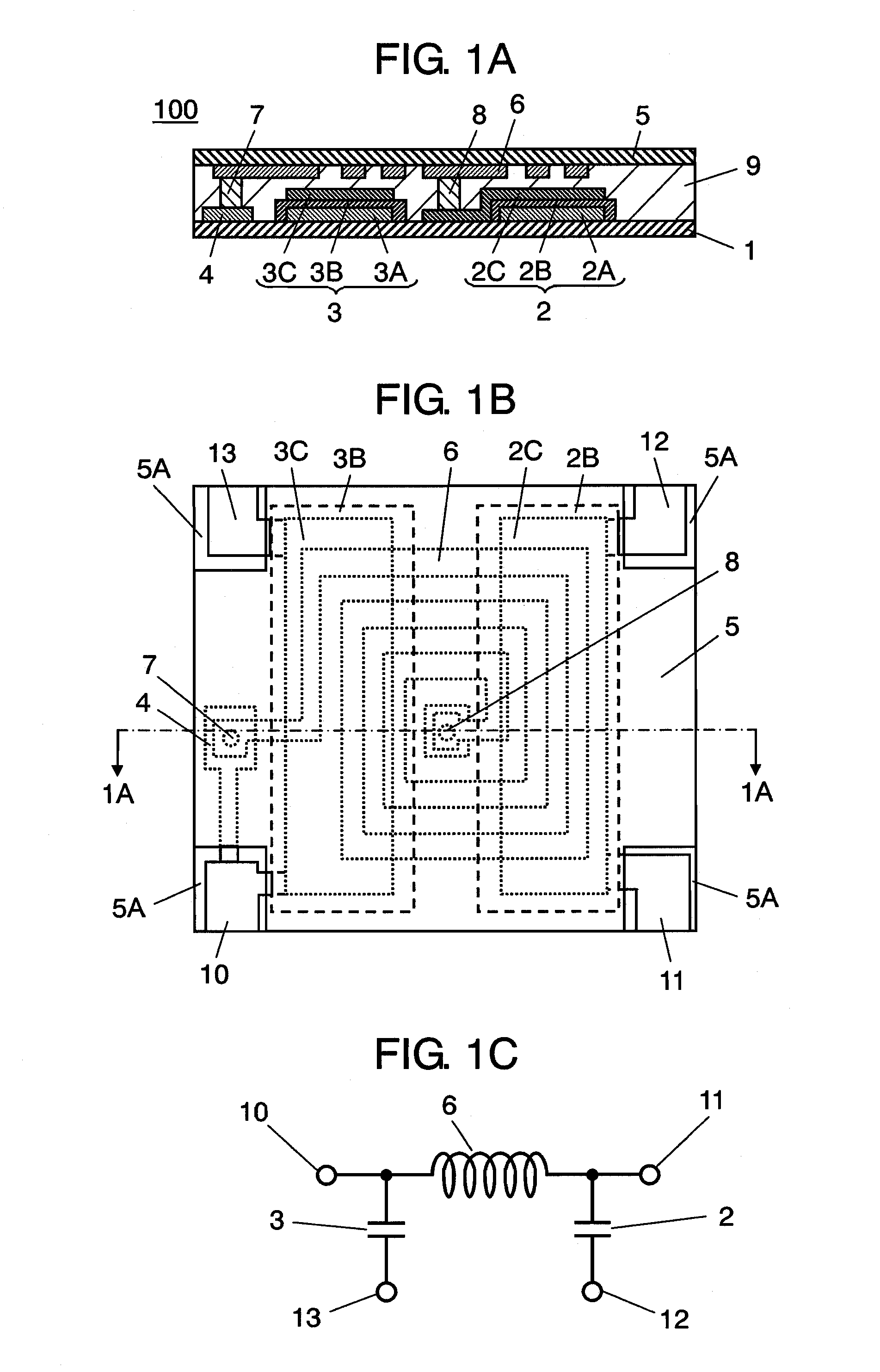
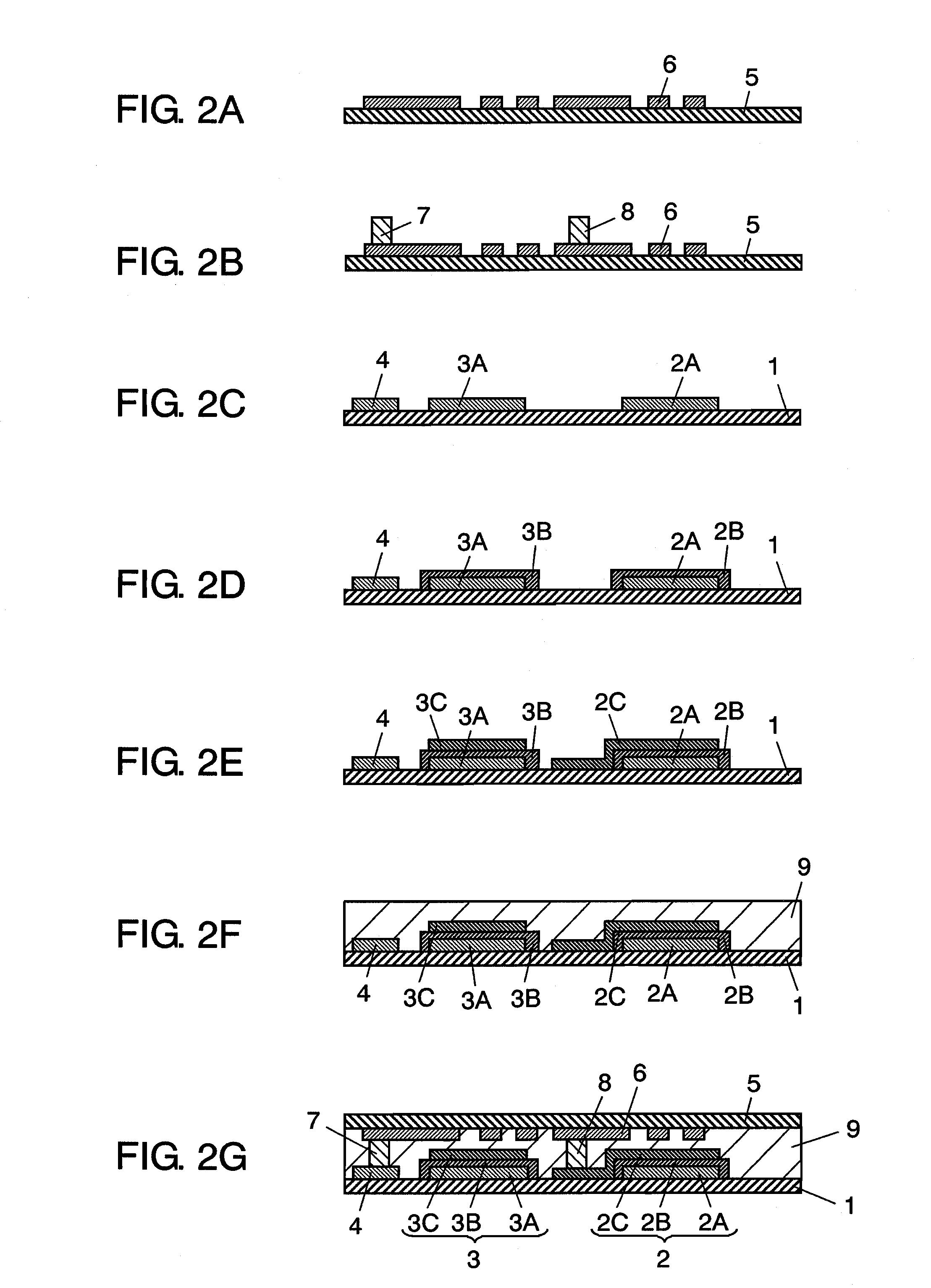
[0085]FIG. 1A to FIG. 1C show the configuration of composite electronic component 100 according to a first embedment of the present invention, and FIG. 1A is a substantial part cross sectional view, FIG. 1B is a plan view, and FIG. 1C is an equivalent circuit diagram. Further, FIG. 1A shows a cross sectional view taken along line 1A-1A of FIG. 1B.

[0086]As shown in FIG. 1A and FIG. 1B, composite electronic component 100 according to the present exemplary embodiment is provided with first sheet substrate 1, second sheet substrate 5, and insulating adhesive resin layer 9 for fixing first sheet substrate 1 to second sheet substrate 5. In first sheet substrate 1, first thin film electronic components 2 and 3 are formed on at least one main face, and external connection terminals 10, 11, 12, and 13 for connecting to the external circuit are formed on this one main face or the other main face. In addition, in second sheet substrate 5, second thin film electronic component 6 is formed on at...

second exemplary embodiment

[0121]FIGS. 4A to 4D show a configuration of composite electronic component 110 according to a second exemplary embodiment of the present invention. The present exemplary embodiment will be described taking the case that the first thin film electronic component is a capacitor element and the second thin film electronic component is an inductor element as an example.

[0122]FIG. 4A is a view showing a cross section along a line 4A-4A of FIG. 4C. However, as described later, FIG. 4C illustrates second sheet substrate 17 merely schematically, so that FIG. 4C is not a precise cross sectional view. FIG. 4B is a plan view showing a configuration of second sheet substrate 17. FIG. 4C is a plan view showing a configuration of first sheet substrate 1, and at the same time, is a view schematically showing electric connection to inductor elements 19 and 20 when second sheet substrate 17 is pasted to first sheet substrate 1. FIG. 4D is an equivalent circuit diagram.

[0123]Composite electronic comp...

third exemplary embodiment

[0154]FIG. 7A is a plan view as seen from the side of second sheet substrate 33 for explaining a configuration of composite electronic component 140 according to a third exemplary embodiment of the present invention. FIG. 7B is a cross sectional view taken along line 7B-7B of FIG. 7A, and FIG. 7C is an equivalent circuit diagram thereof.

[0155]Composite electronic component 140 according to the present exemplary embodiment is configured in such a manner that capacitor element 32 that is first thin film electronic component formed on first sheet substrate 26 is electrically connected to resistor element 31 that is second thin film electronic component formed on second sheet substrate 33 by interlayer connection conductor 37, and first sheet substrate 26 and second sheet substrate 33 are adhered and fixed by insulating adhesive resin layer 36. Hereinafter, first thin film electronic component will be described as capacitor element 32 and second thin film electronic component will be de...


PUM


Abstract

To provide a configuration including a first sheet substrate, on which a first thin film electronic component is formed on at least one main face, and an external connection terminal for connecting to an external circuit is formed one main face or the other face; a second sheet substrate, on which a second thin film electronic component is formed on at least one face; an insulator connection resin layer for fixing the first sheet substrate and the second sheet substrate opposing the first thin film electronic component against the second thin film electronic component; and an interlayer connection conductor for electrically connecting electrode terminals, which have been set in advance, of the first thin film electronic component and the second thin film electronic component.

Description

TECHNICAL FIELD[0001]The present invention relates to a composite electronic component having a plurality of thin film electronic components having different functions mounted on a flexible sheet-like base material, particularly, a sheet-like composite electronic component (hereinafter, referred to as “a composite electronic component”) including thin-type LC circuit and CR circuit, and a method for manufacturing same.BACKGROUND ART[0002]In recent years, in accordance with reduction of a size, reduction of a thickness, and a high performance of a mobile terminal equipment represented by a mobile phone, the further reduction of a thickness and the further reduction of a size of a chip component of an electronic component have been required. However, in mere reduction of a size and mere reduction of a thickness of the chip component, it is expected that there is a very difficulty in a manufacturing step such as mounting of the chip components on a circuit substrate or the like.[0003]O...

Claims


Application Information

Patent Timeline
IPC IPC(8): H03H7/00H05K3/00H05K1/02
CPCH01L23/66Y10T29/49155H03H7/0115H03H7/175H05K1/16H05K1/162H05K1/165H05K3/4614H05K2201/0317H05K2201/086H05K2201/09763H05K2203/1189H01L2924/0002H01L27/016H01L2924/00
Inventor YAMAMOTO, KENICHIKOMYOJI, DAIDOKURAMASU, KEIZABURO
Owner PANASONIC CORP
Why Eureka
Try Eureka