
Delay circuit

a delay circuit and circuit technology, applied in the field of delay circuits, can solve the problems of difficulty in making the delay time more accurate, easy variation of the impedance component, and difficulty in ensuring the accuracy of the delay tim

Inactive Publication Date: 2010-04-15
RENESAS ELECTRONICS CORP
View PDF9 Cites 1 Cited by
  • Summary
  • Abstract
  • Description
  • Claims
  • Application Information

AI Technical Summary

Benefits of technology

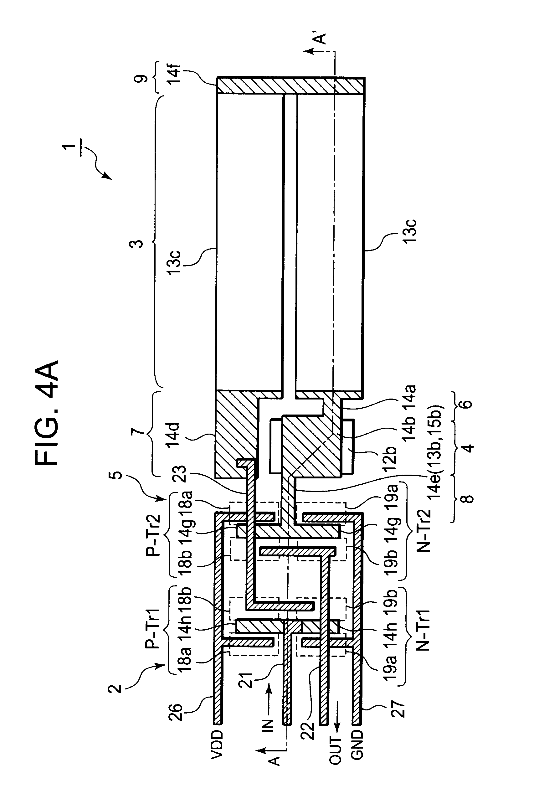
[0011]In the present invention, as the wiring which connects the resistance element (3) and the capacitor element (4), the first silicide layer (14a) is used, and the metal wiring is not used. More specifically, the resistance element (3), the capacitor element (4) and the connection wiring (6) have no metal wirings. Therefore, in these sections, metal wiring coupling noise is not on the delay contact point. Accordingly, propagation of noise can be suppressed. In addition, the metal wiring can be used in the upper layers of them, and metal wiring restriction can be relieved. Further, the first silicide layer (14a) can be formed by being stacked on the film configuring the resistance element (3) and the capacitor element (4). Accordingly, it is not necessary to form a region for a contact as in the case of using a metal wiring, and the areas of the resistance element (3) and the capacitor element (4) can be reduced. More specifically, the circuit area can be reduced. Further, the resistance element (3) and the capacitor element (4) are connected by the connection wiring (6), and therefore, both of them are individually provided. Accordingly, it is considered that by arranging the resistance element (3) at the side near the input, and by arranging the capacitor element (4) at the side near the output, the transistor in the inverter hardly relates to charge and discharge. Accordingly, the delay time can be made more accurate. More specifically, a highly precise delay circuit can be obtained.

Problems solved by technology

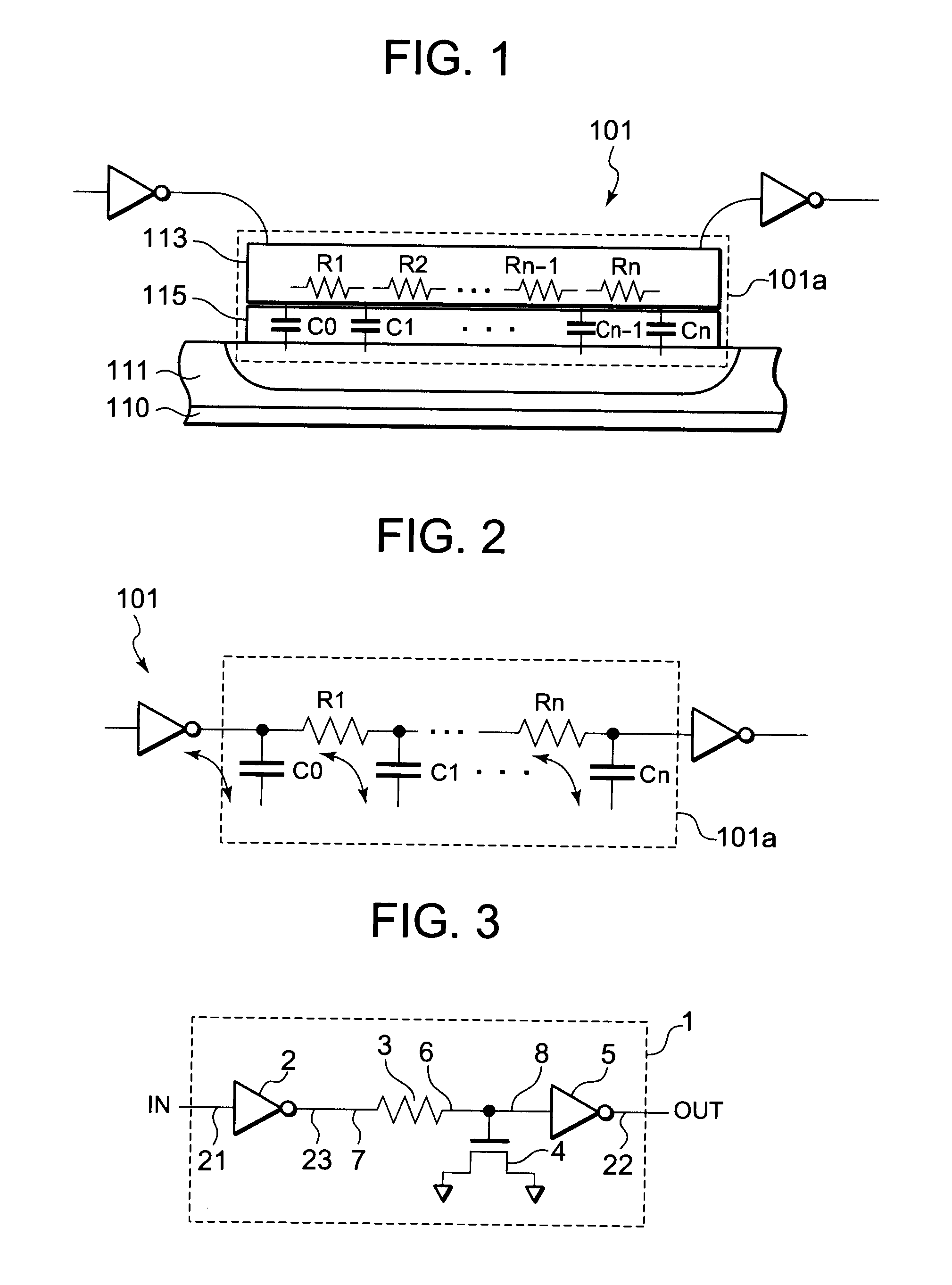
However, in a transistor, variation easily occurs to the impedance component due to the influence of voltage, temperature, a production error and the like as compared with a normal capacitor element and resistance element of simple structures.
Therefore, the delay circuit 101 has difficulty in making the delay time more accurate, and is considered to have a problem of precision.
Accordingly, it is considered to be difficult to realize high size precision.
Therefore, it is conceivable that application of such a gate wiring layer to the resistance element of Japanese Patent Laid-Open No. 2002-94002 makes the resistance value too low.
Further, if metal wiring coupling noise is on a delay contact point, an error occurs.
Therefore, when the metal wiring is used in the delay circuit, there arises the problem of metal wiring restriction which restricts use of the metal wiring in its upper layer.
Further, when a metal wiring is used in the delay circuit, there is the problem of the occurring noise easily propagating to the metal wiring.

Method used


Image

  • Delay circuit
  • Delay circuit
  • Delay circuit

Examples


Embodiment Construction

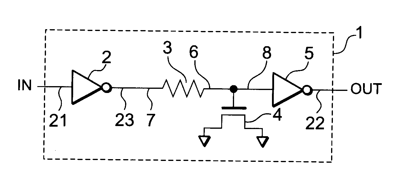
[0020]Hereinafter, a delay circuit according to an embodiment of the present invention will be described with reference to the attached drawings. FIG. 3 is a circuit diagram showing the configuration of the delay circuit according to the embodiment of the present invention. A delay circuit 1 includes an inverter 2, a resistance element 3, a capacitor element 4 and an inverter 5.

[0021]The inverter 2 has an input side connected to a wiring 21 which is a supply source of a signal, and has an output side connected to a wiring 23 which is an output destination of the signal. The wirings 21 and 23 are exemplified by metal wirings. The resistance element 3 has one end connected to the wiring 23, and the other end connected to a wiring 6. The resistance element 3 is exemplified by a polysilicon layer. The wiring 6 is exemplified by a silicide layer (+ a polysilicon layer). The capacitor element 4 has one end connected to the wirings 6 and 8, and the other end buried in a semiconductor subst...


PUM


Abstract

A delay circuit with a delay time being more accurate and a circuit area being reduced is provided. The delay circuit includes a resistance element 3, a capacitor element 4 and a connection wiring 6. The connection wiring 6 includes a first polysilicon layer 13a above a substrate 10, and a first silicide layer 14a which connects the resistance element 3 and the capacitor element 4 and is on the first polysilicon layer 13a. The capacitor element 4 includes a diffusion layer 12b in the surface region of the semiconductor substrate 10, a gate insulating layer 15b on the diffusion layer 12b, a second polysilicon layer 13b on the gate insulating layer 15b, and a second silicide layer 14b on the second polysilicon layer 13b. The resistance element 3 includes a third polysilicon layer 13c above the semiconductor substrate 10. The first, second and third polysilicon layers 13a, 13b and 13c are integrally provided. The first and second silicide layers 14a and 14b are integrally provided.

Description

BACKGROUND OF THE INVENTION[0001]1. Field of the Invention[0002]The present invention relates to a delay circuit, and particularly relates to a delay circuit for use in a semiconductor integrated circuit.[0003]2. Description of the Related Art[0004]In a semiconductor integrated circuit (including a semiconductor memory), a delay circuit which delays a signal by a desired time is used for regulating the timing of propagation of the signal. A delay circuit is generally configured by an inverter, a resistance element, a capacitor element and the like. As a result of enhancement in the operation speed in semiconductor integrated circuits of recent years, extremely high precision is required in regulation of delay times. Therefore, delay circuits need to be manufactured with higher precision so as to obtain more accurate delay times. Further, by microfabrication of a semiconductor integrated circuit, reduction in the circuit area of a delay circuit, and suppression of influence on metal ...

Claims


Application Information

Patent Timeline
IPC IPC(8): H03H11/26H03H7/30H03K5/13
CPCH03H11/26H03H7/30
Inventor TAKAHASHI, HIROYUKI
Owner RENESAS ELECTRONICS CORP
Learn More