ELECTRONIC SEMICONDUCTOR DEVICE BASED ON COPPER NICKEL AND GALLIUM-TIN-ZINC-COPPER-TITANIUM p AND n-TYPE OXIDES, THEIR APPLICATIONS AND CORRESPONDING MANUFACTURE PROCESS

Active Publication Date: 2010-04-15
UNIV NOVA DE LISBOA
View PDF1 Cites 21 Cited by
  • Summary
  • Abstract
  • Description
  • Claims
  • Application Information

AI Technical Summary

Benefits of technology

[0053]The new electronic materials designated by OCuxNiy and GSZTCO, with different compositions, containing or not other impurities like Zirconium or Nitrogen, can be deposited in any type of substrate such as glass, polymer or cellulosic paper, at temperatures below 100° C. Being highly compact / dense, with controlled electrical between 10−14 S.cm−1 to 105 S.cm−1; exhibiting a normal behaviour as p-type material, in the case of OCuxNiy processed at temperatures 100° C. in the presence of a UV light source and n-type, in the case of GSZTCO, can also be converted to p-type by increasing the amount of copper present in the composition or by adding impurities like nitrogen that can substitute one of the elements presents in the GSZTCO composition, such as, Tin or Gallium whose substitution does not bring an enhancement of gaps or interstices in the material allowing a better control concerning the origin of the free carriers, by impurities and not by oxygen vacancies.

Problems solved by technology

Nevertheless, nothing is known about its use as a matching layer.

Method used


Image

  • ELECTRONIC SEMICONDUCTOR DEVICE BASED ON COPPER NICKEL AND GALLIUM-TIN-ZINC-COPPER-TITANIUM p AND n-TYPE OXIDES, THEIR APPLICATIONS AND CORRESPONDING MANUFACTURE PROCESS
  • ELECTRONIC SEMICONDUCTOR DEVICE BASED ON COPPER NICKEL AND GALLIUM-TIN-ZINC-COPPER-TITANIUM p AND n-TYPE OXIDES, THEIR APPLICATIONS AND CORRESPONDING MANUFACTURE PROCESS
  • ELECTRONIC SEMICONDUCTOR DEVICE BASED ON COPPER NICKEL AND GALLIUM-TIN-ZINC-COPPER-TITANIUM p AND n-TYPE OXIDES, THEIR APPLICATIONS AND CORRESPONDING MANUFACTURE PROCESS

Examples


Embodiment Construction

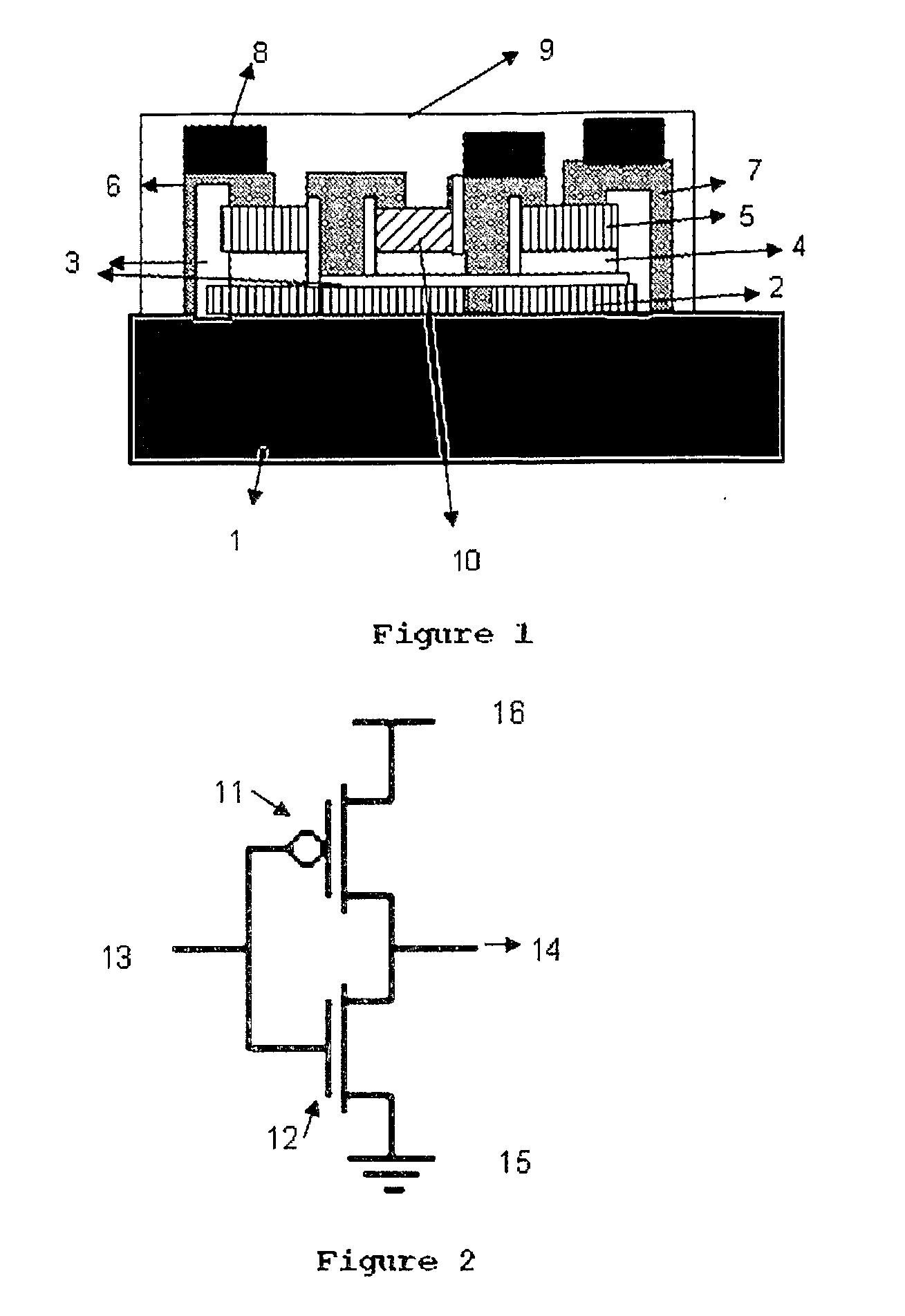
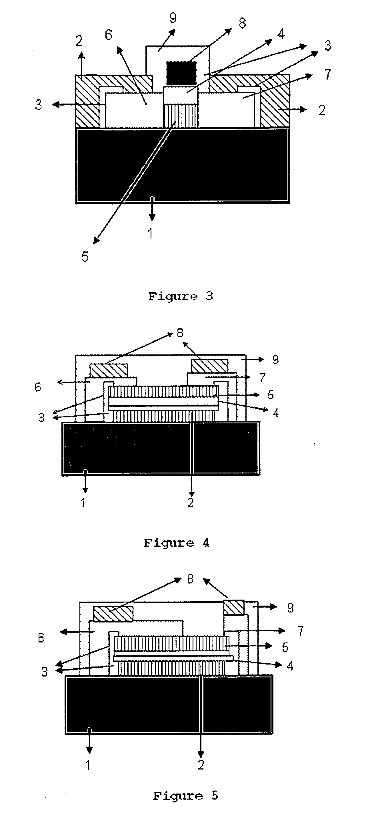
[0086]As previously referred, the main components of the invention are the OCuxNy, see FIGS. 1 and 14, (10), and the GSZTCO, see FIGS. 3, 4 and 14 (4), in their different compositions, including or not impurities, such as, zirconium or nitrogen or molybdenum, according to the percentages already mentioned, p-type and / or n-type; including the use of a tantalum pentoxide matching layer of the active oxide semi-conductor to the dielectric, see for instance, FIGS. 3 and 14 (4) and the encapsulating material, the magnesium fluoride, see FIG. 1, (9).

[0087]The present invention is related to the use of new semiconductors based on multi-component copper and nickel and gallium-tin-zinc-titanium-copper oxides alloy; which is designated as OCuxNiy and GSZTCO; where their component the oxide elements have different compositions as, x which represents the copper molar content, y represents the nickel molar content, m represents the gallium molar contents, n represents the tin molar content, w re...


PUM


Abstract

The present invention corresponds to the use of p and n-type oxide semiconductors based on copper nickel (OCux Niy, with 0<x<3; 0<y<3) or multicomponent Gallium-Tin-Zinc-Copper-Titanium oxide, designated here after as GSZTCO, in different molar compositions, having an amorphous or crystalline structure and with the electrical characteristics of a donor or electron acceptor semiconductor, doped or not doped with impurities, such as, Zirconium or nickel or nitrogen, as a way to control the semiconductor electronic behaviour (valence); including the manufacture process at room temperature or temperatures below 100° C. and their applications in optoelectronic and electronic fields is to manufacture devices, such as, Complementary-Metal-Oxide-Semi-conductors, thin film transistors, pn heterojunctions, logic gates, O-ring oscillators, using as substrate glass, metal foils, polymers or cellulose materials, in which a protection layer based on magnesium fluoride is used, together with a tantalum oxide matching layer of the active semiconductors to a dielectric, such as, silicon dioxide.

Description

FIELD OF INVENTION[0001]The present invent is related to the use of p and n-type oxide semiconductors of copper and nickel (OCuxNiywith 0<x<3; 0<y<3) or multicomponent Gallium-Tin-Zinc-Copper-Titanium, hereafter designated by GSZCTO in different component compositions, having an amorphous or crystalline structure and with the electrical characteristics of a donor (designated by n-type) or electron acceptor (designated by p-type) semiconductor, doped or not doped with impurities such as Zirconium or nickel or nitrogen, as a way to control of the semiconductor electronic behaviour (valence), including the fabrication process at room temperature or temperatures below 100° C. and their applications in optoelectronic and electronic fields to fabricate or produce devices such as Complementary-Metal-Oxide-Semiconductors, C-MOS (FIGS. 1-2), thin film transistors, TFT (FIGS. 3-5), p-n heterojunctions (FIG. 5), logic gates (FIG. 6), O-ring oscillators (FIG. 7), using as substrate ...

Claims


Application Information

Patent Timeline
IPC IPC(8): H01L29/22
CPCH01L21/8252H01L21/8254H01L27/0605H01L29/7869H01L21/02381H01L21/02631H01L21/02425H01L21/02554H01L21/02565H01L21/02581H01L21/02422
Inventor FERRAO DE PAIVA MARTINS, RODRIGOCORREIA FORTUNATO, ELVIRA MARIA
Owner UNIV NOVA DE LISBOA
Why Eureka
Try Eureka