Magnetoresistive effect device and magnetic memory
a magnetic memory and magnetoresistive effect technology, applied in solid-state devices, magnetic bodies, instruments, etc., can solve the problems of requiring a greater magnetic field, and reducing the current flow through the wiring, so as to minimize the leakage magnetic field
- Summary
- Abstract
- Description
- Claims
- Application Information
AI Technical Summary
Benefits of technology
Problems solved by technology
Method used
Image
Examples
first embodiment
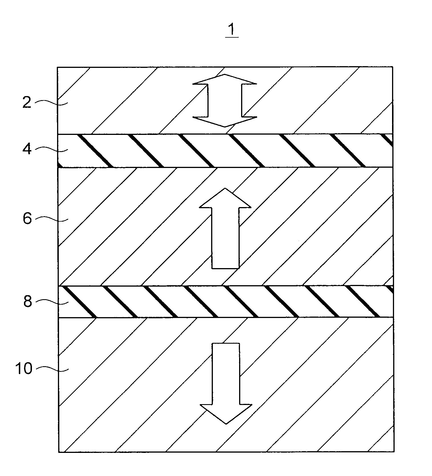
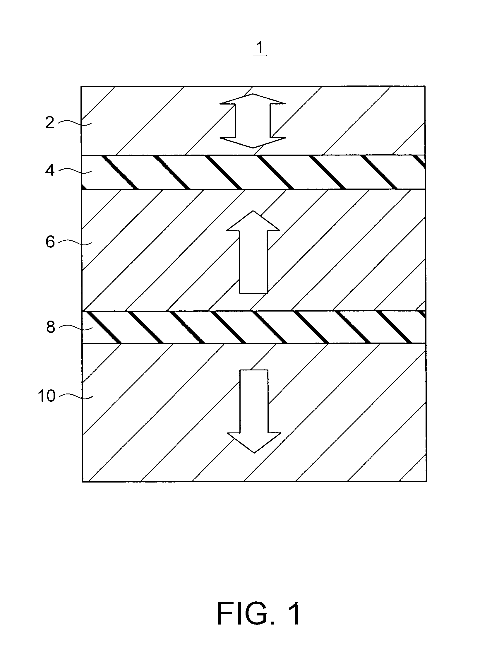
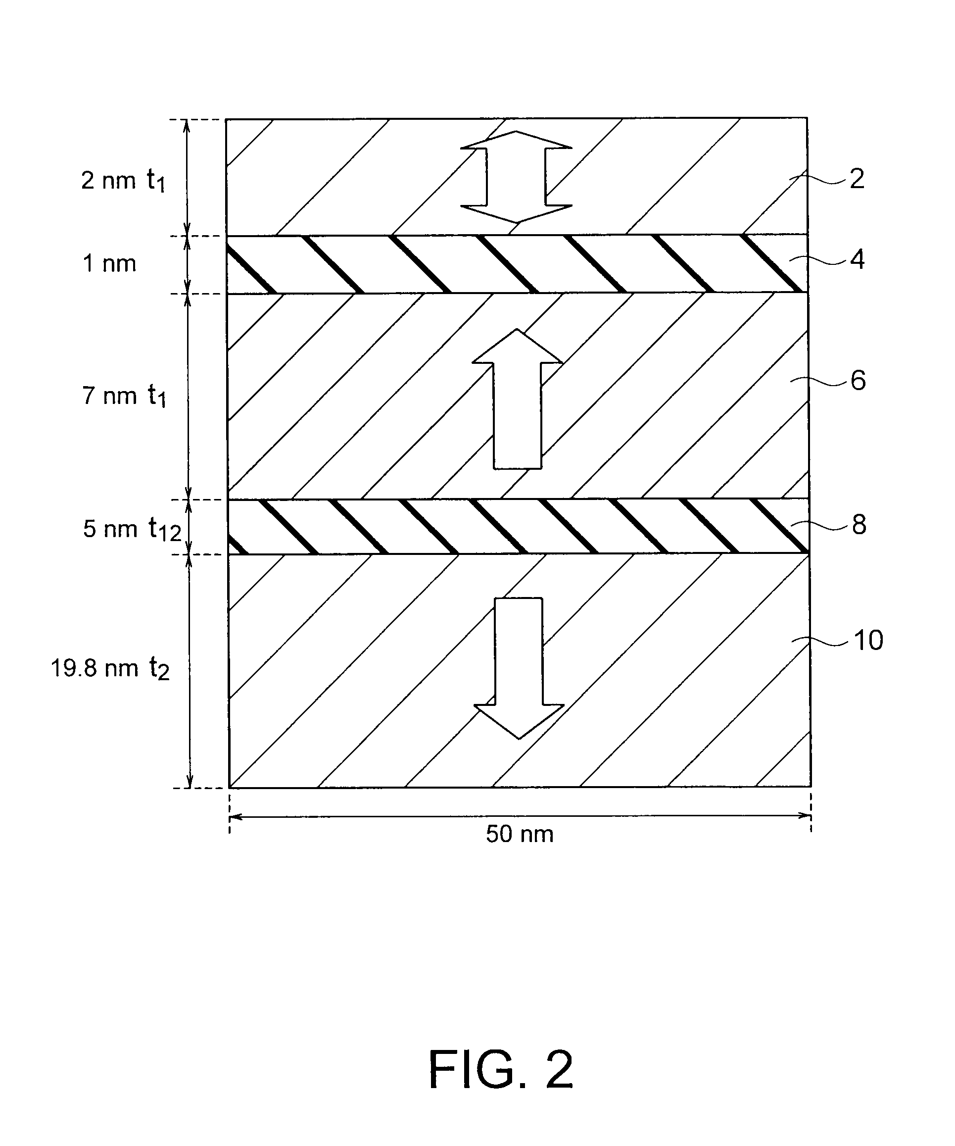
[0049]FIG. 1 shows a magnetoresistive effect device in accordance with a first embodiment of the present invention. The magnetoresistive effect device of this embodiment is a MTJ device 1 of a single-pin structure. The MTJ device 1 of this embodiment has a stacked structure that includes a free magnetization layer (a storage layer) 2 formed with a magnetic layer, a reference layer 6 formed with a magnetic layer, a ferromagnetic layer 10 formed with a magnetic layer, a nonmagnetic layer 4 interposed between the storage layer 2 and the reference layer 6, and a nonmagnetic layer 8 interposed between the reference layer 6 and the ferromagnetic layer 10. Accordingly, the MTJ device 1 of this embodiment may be a stacked structure formed by stacking the ferromagnetic layer 10, the nonmagnetic layer 8, the reference layer 6, the nonmagnetic layer 4, and the storage layer 2 in this order (the stacked structure formed in the order illustrated in FIG. 1), or may be a stacked structure formed b...
second embodiment
[0111]FIG. 11 shows a magnetoresistive effect device in accordance with a second embodiment of the present invention. The magnetoresistive effect device of this embodiment is a MTJ device 1 of a dual-pin structure. The MTJ device 1 of this embodiment has a stacked structure that is formed by stacking a ferromagnetic layer 12, a nonmagnetic layer 14, a reference layer 16, a nonmagnetic layer 18, a storage layer 20, a nonmagnetic layer 22, a reference layer 24, a nonmagnetic layer 26, and a ferromagnetic layer 28 in this order. Alternatively, the MTJ device 1 of this embodiment may have a stacked structure that is formed by stacking the ferromagnetic layer 28, the nonmagnetic layer 26, the reference layer 24, the nonmagnetic layer 22, the storage layer 20, the nonmagnetic layer 18, the reference layer 16, the nonmagnetic layer 14, and the ferromagnetic layer 12 in this order, which is the reverse order of the order illustrated in FIG. 11.
[0112]The reference layers 16 and 24, the ferro...
third embodiment
[0137]FIG. 13 shows a magnetoresistive effect device in accordance with a third embodiment of the present invention. The magnetoresistive effect device of this embodiment is a MTJ device 1 of a single-pin structure. The MTJ device 1 of this embodiment has a stacked structure that includes a storage layer 102 formed with a magnetic layer, a reference layer 106 formed with a magnetic layer, a ferromagnetic layer 110 formed with a magnetic layer, a nonmagnetic layer 104 interposed between the storage layer 102 and the reference layer 106, and an antiferromagnetic layer 108 interposed between the reference layer 106 and the ferromagnetic layer 110. Accordingly, the MTJ device 1 of this embodiment may be a stacked structure formed by stacking the storage layer 102, the nonmagnetic layer 104, the reference layer 106, the antiferromagnetic layer 108, and the ferromagnetic layer 110 in this order (the stacked structure formed in the order illustrated in FIG. 13), or may be a stacked structu...
PUM
 Abstract
Description
Claims
Application Information
 - R&D
- Intellectual Property
- Life Sciences
- Materials
- Tech Scout
- Unparalleled Data Quality
- Higher Quality Content
- 60% Fewer Hallucinations
Browse by: Latest US Patents, China's latest patents, Technical Efficacy Thesaurus, Application Domain, Technology Topic, Popular Technical Reports.
© 2025 PatSnap. All rights reserved.Legal|Privacy policy|Modern Slavery Act Transparency Statement|Sitemap|About US| Contact US: help@patsnap.com


