Spin transistor, integrated circuit, and magnetic memory

a technology of integrated circuits and pin transistors, applied in semiconductor devices, digital storage, instruments, etc., can solve problems such as deterioration of idp/idap ratio

Inactive Publication Date: 2010-03-25
KK TOSHIBA
View PDF12 Cites 18 Cited by
  • Summary
  • Abstract
  • Description
  • Claims
  • Application Information

AI Technical Summary

Benefits of technology

[0009]A spin transistor of an aspect of the present invention comprises a first ferromagnetic layer, a second ferromagnetic layer, a semiconductor layer between the first and second ferromagnetic layers, and a gate electrode on or above a surface of the semiconductor layer, the surface being between the first and second ferromagnetic layers. One of the first and second ferromagnetic layers has an invariable magnetization and the other has a variable magnetization. Data are stored by a relation of magnetization directions of the first and second ferromagnetic layers. Electrons flow from the first ferromagnetic layer to the second ferromagnetic layer in a read operation. And The first ferromagnetic layer comprises a ferromagnet which has a first minority spin band located at a high energy side and a second minority spin band located at a low energy side, and has a Fermi level in an area of the high energy side higher than a middle of a gap between the first and second minority spin bands.

Problems solved by technology

However, even if the magnetic material having the spin polarization ratio of 100% can be used, unfortunately the IDP / IDAP ratio is deteriorated when a finite bias voltage is applied between the source electrode and drain electrodes.

Method used


Image

  • Spin transistor, integrated circuit, and magnetic memory
  • Spin transistor, integrated circuit, and magnetic memory
  • Spin transistor, integrated circuit, and magnetic memory

Examples


first embodiment

(1) First Embodiment

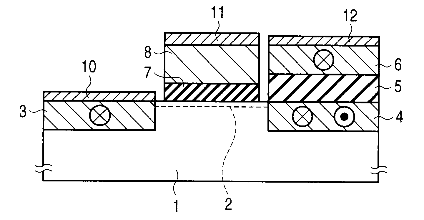
[0124]FIG. 8 is a spin transistor according to a first embodiment of the invention.

[0125]The spin transistor of the first embodiment has the MOSFET structure.

[0126]Two recesses are made in a surface of a semiconductor substrate 1, one of the recesses is filled with a ferromagnetic layer 3, and another recess is filled with a ferromagnetic layer 4. A gate electrode 8 is formed on a channel 2 between the ferromagnetic layers 3 and 4 while a gate insulator 7 is interposed between the gate electrode 8 and the channel 2.

[0127]The ferromagnetic layer 3 is a magnetic pinned layer whose magnetization direction is invariable, and the ferromagnetic layer 4 is a magnetic free layer whose magnetization direction is variable. A ferromagnetic layer 6 is formed on the ferromagnetic layer 4 with a non-magnetic layer 5 interposed therebetween. The non-magnetic layer 5 may be either an insulating material or a conductive material. The ferromagnetic layer 6 is the magnetic pinned l...

second embodiment

(2) Second Embodiment

[0148]FIG. 9 is a spin transistor according to a second embodiment of the invention.

[0149]The spin transistor of the second embodiment has the J-FET structure or MESFET structure.

[0150]In the J-FET structure, the gate electrode 8 is made of a semiconductor, and the conduction type of the gate electrode 8 is opposite to the conduction type of the semiconductor substrate 1. In the MESFET structure, the gate electrode 8 is made of metal. In the MESFET structure, the semiconductor substrate 1 is mainly made of a compound semiconductor (such as GaAs, InP, and SiC), and a Schottky junction is formed by the semiconductor substrate 1 and the gate electrode 8.

[0151]Two recesses are made in the surface of the semiconductor substrate 1, one of the recesses is filled with the ferromagnetic layer 3, and the other recess is filled with the ferromagnetic layer 4. The gate electrode 8 is formed on the channel 2 between the ferromagnetic layers 3 and 4.

[0152]The ferromagnetic la...

third embodiment

(3) Third Embodiment

[0169]FIG. 10 is a spin transistor according to a third embodiment of the invention.

[0170]The spin transistor of the third embodiment has the MOSFET structure. The spin transistor of the third embodiment is a modification of the spin transistor of the first embodiment.

[0171]The spin transistor of the third embodiment differs from the spin transistor of the first embodiment in that an anti-ferromagnetic layer AF1 is disposed between the ferromagnetic layer 3 and electrode 10 while an anti-ferromagnetic layer AF2 is disposed between the ferromagnetic layer 6 and the electrode 12. The anti-ferromagnetic layers AF1 and AF2 are also called a pinned layer, and the anti-ferromagnetic layers AF1 and AF2 have functions of pinning the magnetization of the ferromagnetic layers 3 and 6 that are of the magnetic pinned layers.

[0172]Due to the existence of the anti-ferromagnetic layers AF1 and AF2, the magnetization directions of the ferromagnetic layers 3 and 6 are stabilized ...


PUM


Abstract

A spin transistor includes a first ferromagnetic layer, a second ferromagnetic layer, a semiconductor layer between the first and second ferromagnetic layers, and a gate electrode on or above a surface of the semiconductor layer, the surface being between the first and second ferromagnetic layers. The first ferromagnetic layer comprises a ferromagnet which has a first minority spin band located at a high energy side and a second minority spin band located at a low energy side, and has a Fermi level in an area of the high energy side higher than a middle of a gap between the first and second minority spin bands.

Description

CROSS-REFERENCE TO RELATED APPLICATIONS[0001]This application is based upon and claims the benefit of priority from prior Japanese Patent Application No. 2008-244760, filed Sep. 24, 2008, the entire contents of which are incorporated herein by reference.BACKGROUND OF THE INVENTION[0002]1. Field of the Invention[0003]The present invention relates to a spin transistor, an integrated circuit, and a magnetic memory.[0004]2. Description of the Related Art[0005]Recently, new devices in which behaviors of a charge and a spin of an electron are simultaneously utilized, are being increasingly developed. Among others, in a spin transistor, ferromagnetic materials are used as a source electrode and a drain electrode, and an output characteristic is controlled by changing relative magnetization directions of the source electrode and drain electrode (for example, see S. Sugahara and M. Tanaka, Appl. Phys. Lett. 84 (2004) 2307, G. H. Fecher and C. Felser, J. Phys. D40, 1582 (2007), B. Balke et. a...

Claims


Application Information

Patent Timeline
Patent Type & Authority Applications(United States)
IPC IPC(8): H01L29/82
CPCH01L29/66984G11C11/16G11C11/161G11C11/1673G11C11/1675G11C11/1693
Inventor INOKUCHI, TOMOAKIMARUKAME, TAKAOISHIKAWA, MIZUESUGIYAMA, HIDEYUKISAITO, YOSHIAKI
Owner KK TOSHIBA
Why Eureka
Try Eureka