
Non-volatile sonos-type memory device

a memory device and non-volatile technology, applied in the field of semiconductor devices, can solve the problems of difficult to reduce a cell portion, increase in manufacturing costs, and limit the design of flash memory with floating gate technique, and achieve the effect of easy data erase and high data retention characteristics

Active Publication Date: 2010-01-28
MONTEREY RES LLC
View PDF12 Cites 2 Cited by
  • Summary
  • Abstract
  • Description
  • Claims
  • Application Information

AI Technical Summary

Benefits of technology

"The present invention provides a technique for forming a non-volatile memory of the SONOS type with excellent data retention characteristics and easy data deletion. This is achieved by using a high-concentration impurity region of the same conductivity type as the semiconductor substrate, which makes it easy to delete data. The charge storage region includes a tunnel oxide film and a storage film provided below a word line and above the semiconductor substrate, assist gates provided on a gate insulating film on the semiconductor substrate, and a substantially U-shaped recess in the semiconductor substrate located between adjacent assist gates. The tunnel oxide film has a thickness of 4 nm or more, which ensures FN tunneling is dominant. The semiconductor device may also include sidewalls along sides of the assist gates and a substantially U-shaped recess in the semiconductor substrate."

Problems solved by technology

However, there are limitations for flash memory designed with the floating gate technique if the memory cell is further downsized to realize high storage density in the flash memory and the manufacturing process rule becomes equal to or smaller than 90 nm.
This is because the area of the high-voltage transistor-forming region, to be provided for programming and erasing data, inevitably becomes relatively wide in a small-sized memory of the floating gate type, resulting in a rise in the manufacturing costs, or it becomes difficult to reduce a cell portion without degrading the reliability due to the possibility of memory error or data loss.
This makes it difficult to downsize the width of the diffusion layer to the limit of the photolithography technique.
Moreover, if a self-alignment process with the use of a hard mask is employed by providing a sidewall to overcome the aforementioned limitation in the photolithography technique, the device fabrication process will become complicated.

Method used


Image

  • Non-volatile sonos-type memory device
  • Non-volatile sonos-type memory device
  • Non-volatile sonos-type memory device

Examples


first embodiment

[0079]In the present embodiment, there is provided an ONO structure in which a tunnel oxide film, a storage nitride film, and a top oxide film are sequentially laminated. This ONO structure is formed after the assist gate is formed, and there is not provided a sidewall on a side wall of the assist gate.

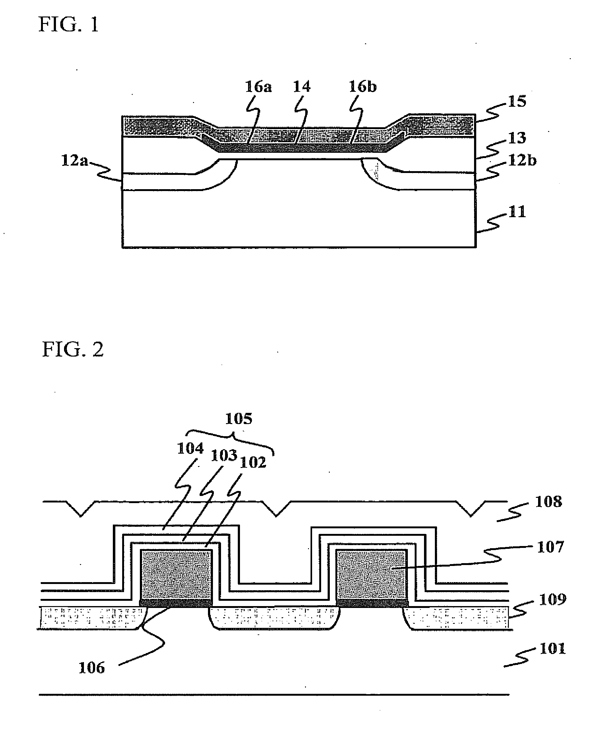
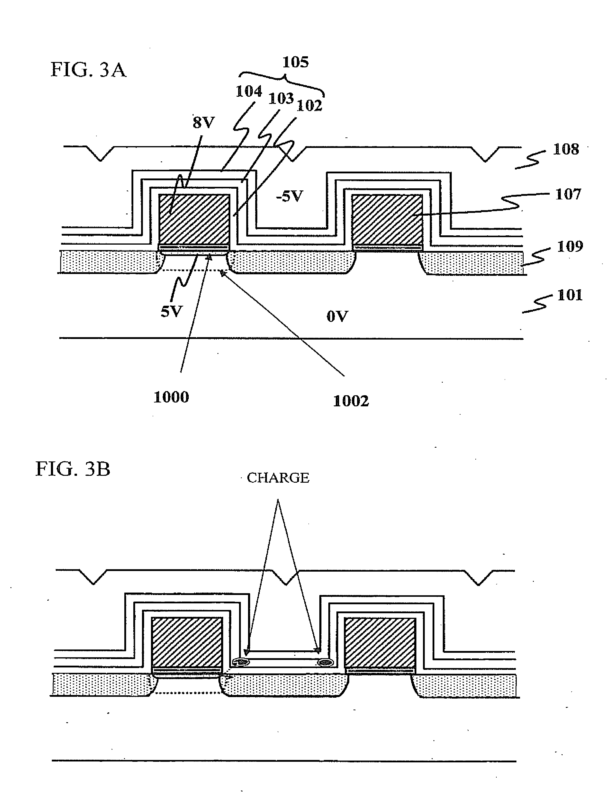
[0080]FIG. 2 is a view illustrating a cross-sectional view of the memory cell in accordance with a first embodiment of the present invention. In this figure, a reference numeral 101 represents a semiconductor substrate, a reference numeral 102 represents a tunnel oxide film, a reference numeral 103 represents a storage film of silicon nitride film, and a reference numeral 104 represents a top oxide film provided on the storage film 103. A laminated structure of the tunnel oxide film 102, the storage film 103, and the top oxide film 104 forms an ONO structure 105. As described above, both the tunnel film 102 and the top film 104 are configured to be oxide films having thicknesses at le...

second embodiment

[0087]In regards to the next embodiment, there is provided the ONO structure in which the tunnel oxide film, the storage nitride film, and the top oxide film are sequentially laminated. This ONO structure is formed after the assist gate is formed, and there is not provided a sidewall on a side wall of the assist gate. In addition, the surface region of the semiconductor substrate is cut out in a U shape between the assist gates.

[0088]FIG. 13 is a cross-sectional view illustrating a-memory cell in accordance with a second embodiment of the present invention. In this figure, the same components and configurations as those of FIG. 2 have the same reference numerals. Also in the second embodiment, both the tunnel film 102 and the top film 104 are configured to be the oxide films having thicknesses equal to or greater than 4 nm, which is equal to the thickness of the FN tunneling region.

[0089]In the second embodiment, there is provided the U-shaped cutout between the assist gates adjacen...

third embodiment

[0094]In the next embodiment (the third embodiment), there is provided the ONO structure in which the tunnel oxide film, the storage nitride film, and the top oxide film are sequentially laminated. This ONO structure is formed before the assist gate is formed, and there is not provided a sidewall on a side wall of the assist gate.

[0095]FIG. 22 is a cross-sectional view illustrating a memory cell in accordance with a third embodiment of the present invention. In this figure, the same components and configurations as those of FIG. 2 have the same reference numerals. The assist gate 107 is formed on the ONO structure 105, which is formed on the surface of the semiconductor substrate 101. A reference numeral 111 shown in this figure is an insulating film formed on the top and side walls of the assist gate 107.

[0096]In this configuration, the tunnel oxide film 102 included in the ONO structure 105 also serves as a gate insulating film of the assist gate 107. Here, both the tunnel film 10...


PUM


Abstract

A semiconductor memory device with the thickness of both a tunnel film and a top film provided thereon configured to be in the FN tunneling region (4 nm or more). Data retention characteristics can be improved by configuring both a tunnel film and a top film to have a thickness in the FN tunneling region. Secondly, a high-concentration impurity region of a conductivity type the same as that of the substrate is provided in a substrate region arranged between assist gates provided adjacently to each other. The aforementioned high-concentration impurity region makes a depletion layer extremely thin when bias is applied to the assist gates. Hot holes generated between bands in the depletion region are injected into a charge storage region and the holes and electrons make pairs and disappear, enabling easy data erasing.

Description

CROSS-REFERENCES TO RELATED APPLICATIONS[0001]This is a divisional of U.S. patent application Ser. No. 11 / 319,999, filed Dec. 27, 2005, which is a continuation of International Application No. PCT / JP2004 / 019647, filed Dec. 28, 2004, which was not published in English under PCT Article 21(2).TECHNICAL FIELD[0002]This invention generally relates to semiconductor devices, and more particularly, to a non-volatile SONOS-type memory technology, which enables excellent data retention characteristics and easy data erase.BACKGROUND[0003]Conventionally, flash memories with the use of the floating gate technique have been widely used as non-volatile flash memories to be incorporated into the electronics devices. However, there are limitations for flash memory designed with the floating gate technique if the memory cell is further downsized to realize high storage density in the flash memory and the manufacturing process rule becomes equal to or smaller than 90 nm. This is because the area of t...

Claims


Application Information

Patent Timeline
Patent Type & Authority Applications(United States)
IPC IPC(8): H01L21/28
CPCH01L21/28282H01L27/115H01L29/792H01L29/66833H01L27/11568H01L29/40117H10B43/30H10B69/00G11C16/0491
Inventor NANSEI, HIROYUKI
Owner MONTEREY RES LLC
Learn More