
Solution processable material for electronic and electro-optic applications

Active Publication Date: 2010-01-21
SOLARMER ENERGY INC
View PDF11 Cites 44 Cited by
  • Summary
  • Abstract
  • Description
  • Claims
  • Application Information

AI Technical Summary

Benefits of technology

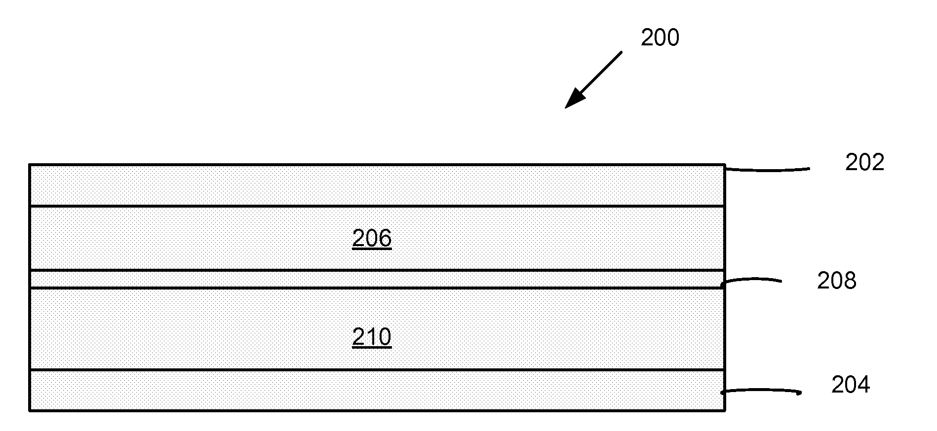
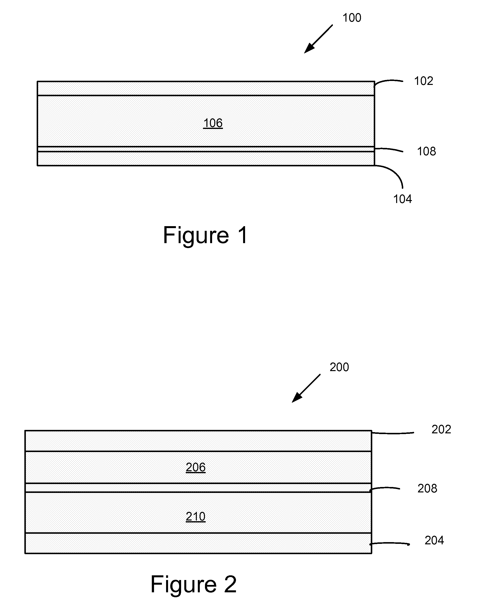
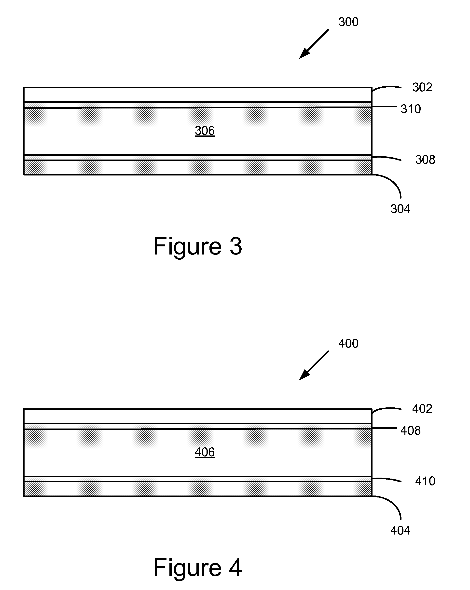
[0013]An electro-optic device according to an embodiment of the current invention has a first electrode, a second electrode spaced apart from the first electrode, an active layer disposed between the first electrode and the second electrode, and an interfacial layer in contact with the active layer. The interfacial layer comprises a blend of a metal oxide and a salt according to an embodiment of the current invention. The interfacial layer comprises a blend of a metal oxide and a second material that at least one of reduces a work function or increases an electrical conductivity of the interfacial layer according to an embodiment of this invention.
[0014]A method of producing an electro-optic device according to an embodiment of the current invention includes forming an active polymer layer, and forming an interfacial layer on a surface of said active polymer layer. Forming the interfacial layer includes forming the interfacial layer from a blend of a metal oxide and a salt according to an embodiment of the current invention. Forming the interfacial layer includes forming the interfacial layer from a blend of a metal oxide and a second material that at least one of reduces a work function or increases an electrical conductivity of the interfacial layer according to an embodiment of this invention.

Problems solved by technology

However, efficient crystalline-based devices, especially of large surface area, are difficult and expensive to produce due to the problems inherent in producing large crystals without significant efficiency-degrading defects.
On the other hand, high efficiency amorphous silicon devices still suffer from problems with stability.
The maximum total power generated by a PV device is inherently incapable of exceeding the product ISC×VOC.
Either of these outcomes is undesirable in a PV device.
The result is that device configuration predictions from donor / acceptor criteria may not be borne out by actual device performance.
However, organic PV devices typically have relatively low quantum yield (the ratio of photons absorbed to carrier pairs generated, or electromagnetic radiation to electricity conversion efficiency), being on the order of 1% or less.
However, the diffusion length (LD) of an exciton is typically much less than the optical absorption length, requiring a trade off between using a thick, and therefore resistive, cell with multiple or highly folded interfaces, or a thin cell with a low optical absorption efficiency.

Method used


Image

  • Solution processable material for electronic and electro-optic applications
  • Solution processable material for electronic and electro-optic applications
  • Solution processable material for electronic and electro-optic applications

Examples


examples

[0044]According to an embodiment of the current invention, we provide a method to make efficient organic electronic devices by utilizing a mixture of solution processable semiconducting metal oxides and salts to form functional interfacial layers in polymer electronics. One example is an anatase TiO2 and Cs2CO3 blend. Introducing a nano-scale TiO2 and Cs2CO3 interfacial layer can provide solar cell performance as good as a device with a low work-function metal Ca as an electrode which is easy to be oxidized (Greczynski, G.; Kugler, T.; Keil, M.; Osikowicz, W.; Fahlman, M.; Salaneck, W. R. J. Electron Spectrosc. Relat. Phenom. 2001, 121, 1). The effectiveness of this unique approach is expanded to polymer LEDs in other particular embodiments of this invention where a lower driving voltage, improved efficiency and extended lifetime are again demonstrated.

[0045]Semiconducting TiO2 has been extensively studied as a promising material in a variety of applications including dye-sensitized...


PUM

PropertyMeasurementUnit
Electrical conductivityaaaaaaaaaa
Volumeaaaaaaaaaa
Ratioaaaaaaaaaa

Abstract

An electro-optic device has a first electrode, a second electrode spaced apart from the first electrode, an active layer disposed between the first electrode and the second electrode, and an interfacial layer in contact with the active layer. The interfacial layer is a blend of a metal oxide and a second material that at least one of reduces a work function or increases an electrical conductivity of the interfacial layer according to an embodiment of this invention. A composition for electro-optic devices is a blend of at least one metal oxide and at least one salt in a ratio, by volume, of at least 1:0.1 and less than 1:1.2.

Description

BACKGROUND[0001]1. Field of Invention[0002]Embodiments of this invention relate to materials for electro-optic devices, electro-optic devices that use the materials and methods of producing the materials and electro-optic devices. More particularly, embodiments of this invention relate to materials for electro-optic devices that are blends of a metal oxide and at least one other material that increases electrical conductivity and / or decreases a work function of a layer of such a material when blended with the metal oxide, to electro-optic devices that use the materials and methods of producing the materials and electro-optic devices.[0003]2. Discussion of Related Art[0004]The contents of all references referred to herein, including articles, published patent applications and patents are hereby incorporated by reference.[0005]Electronic devices based on organic materials (small molecules and polymers) have attracted broad interest. Such devices include organic light emitting devices ...

Claims


Application Information

Patent Timeline
IPC IPC(8): H01L31/00H01B1/00
CPCB82Y10/00H01B1/08H01L51/0036Y02E10/549H01L51/0047H01L51/4253H05B33/26H01L51/0038H10K85/113H10K85/114H10K85/215H10K30/30H10K30/50
Inventor YANG, YANGPARK, MI-HYAELI, GANG
Owner SOLARMER ENERGY INC
Learn More