Copper Sputtering Target With Fine Grain Size And High Electromigration Resistance And Methods Of Making the Same
- Summary
- Abstract
- Description
- Claims
- Application Information
AI Technical Summary
Benefits of technology
Problems solved by technology
Method used
Image
Examples
Embodiment Construction
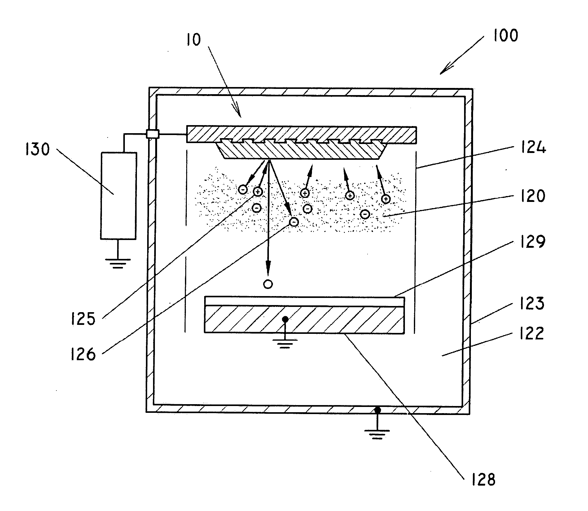
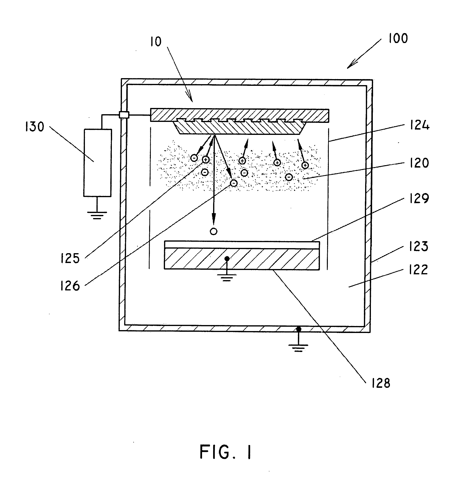
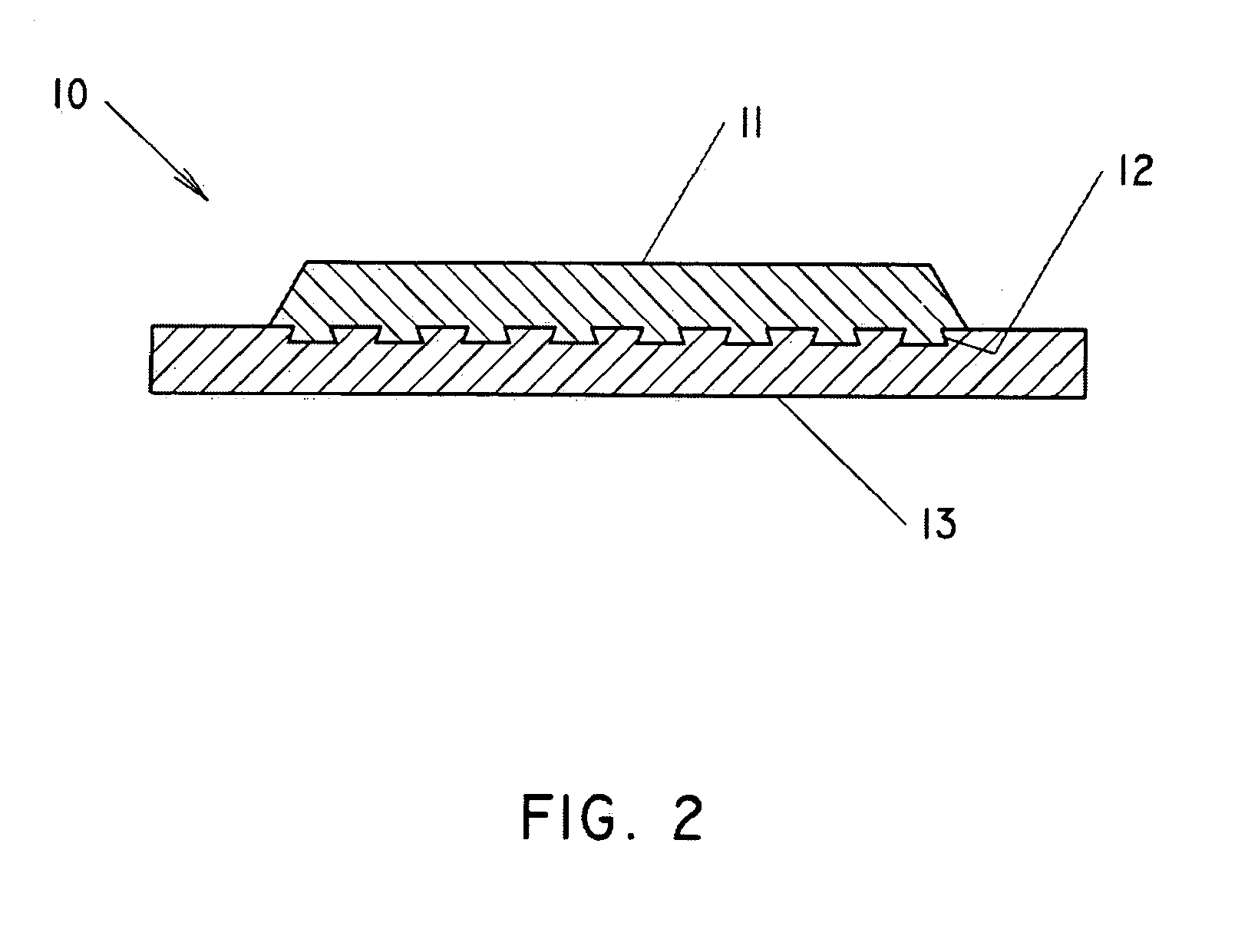
[0019]The copper sputtering target encompassed by this invention can have any suitable geometry, and can be bonded to the backing plate 13 or monolithic. The bond 12 can be either solder bond or Tosoh SMD patented Forte® bond as set forth in U.S. Pat. No. 6,749,103, incorporated by reference herein. The target encompassed by this invention can be applied in any suitable sputtering apparatus including, but not limited to the apparatus with reference to FIG. 1.
[0020]The present invention includes methods of manufacturing the copper target containing one or more of other alloying elements including Al, Ag, Co, Cr, Ir, Fe, Mo, Ti, Pd, Ru, Ta, Sc, Hf, Zr, V, Nb, Y, and rare earth metals. The copper raw material will preferably have a purity of at least 99.9995 wt %. The alloying elements may have lower purity, for example, the iridium raw material will preferably have a purity of 99.5 wt %. The titanium raw material will preferably have a purity of 99.995 wt %. The palladium raw material...
PUM
| Property | Measurement | Unit |
|---|---|---|
| Grain size | aaaaa | aaaaa |
| Temperature | aaaaa | aaaaa |
| Temperature | aaaaa | aaaaa |
Abstract
Description
Claims
Application Information
 - R&D
- Intellectual Property
- Life Sciences
- Materials
- Tech Scout
- Unparalleled Data Quality
- Higher Quality Content
- 60% Fewer Hallucinations
Browse by: Latest US Patents, China's latest patents, Technical Efficacy Thesaurus, Application Domain, Technology Topic, Popular Technical Reports.
© 2025 PatSnap. All rights reserved.Legal|Privacy policy|Modern Slavery Act Transparency Statement|Sitemap|About US| Contact US: help@patsnap.com


