
Method of manufacturing semiconductor device and substrate processing apparatus

a technology of substrate processing and manufacturing method, which is applied in the direction of semiconductor devices, chemical vapor deposition coatings, coatings, etc., can solve the problems of increasing eot, flatness of film, and the impurity residue of precursors cannot be completely removed, so as to improve the overall film formation rate of metal composite films, improve the throughput, and improve the effect of film formation ra

Active Publication Date: 2009-12-31
KOKUSA ELECTRIC CO LTD
View PDF4 Cites 30 Cited by
  • Summary
  • Abstract
  • Description
  • Claims
  • Application Information

AI Technical Summary

Benefits of technology

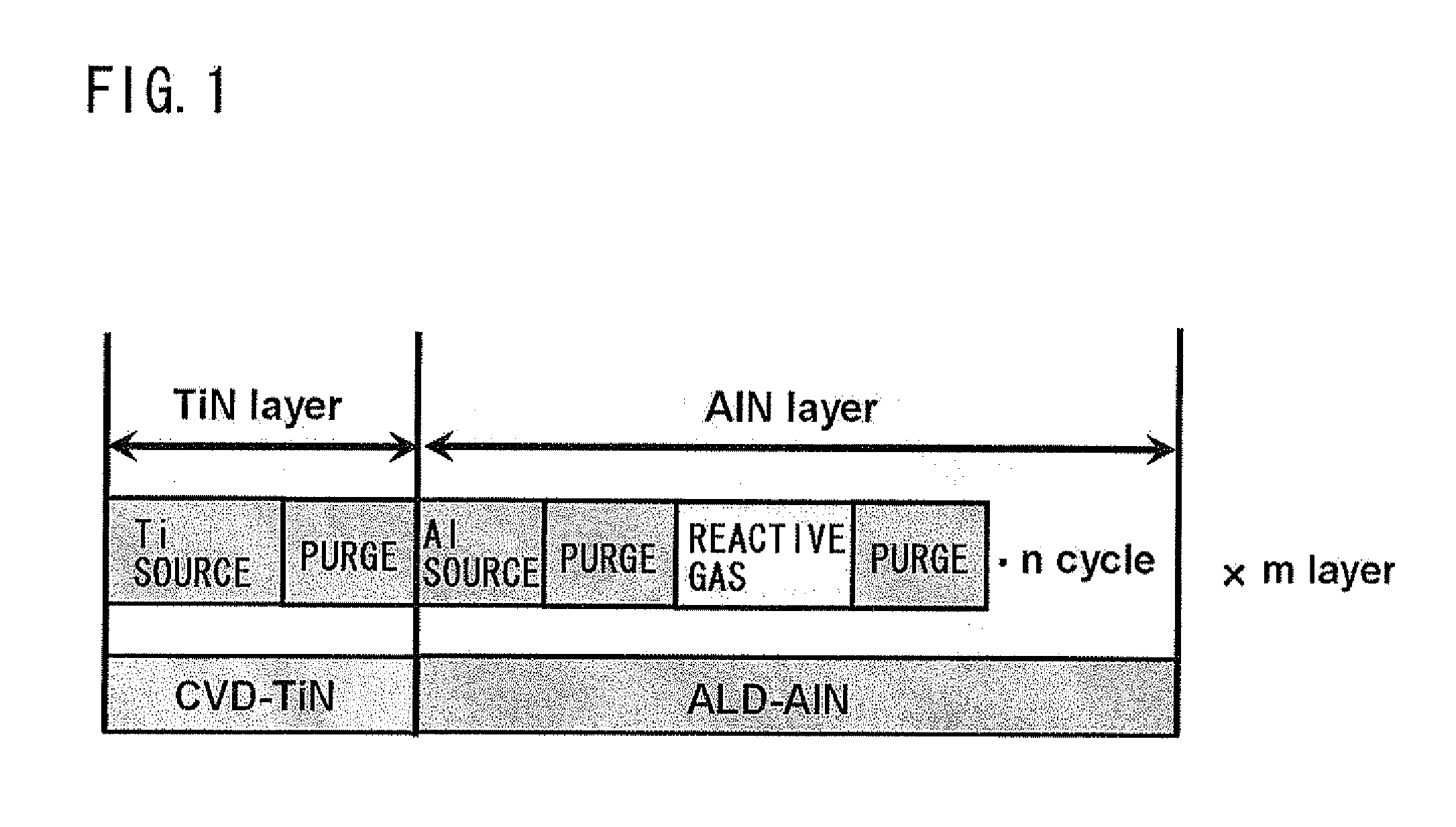
[0099]According to this embodiment, the first metal film (TiN film), becoming a base of the metal composite film (TiAlN film) is formed by CVD method. Therefore, a total film formation rate of the metal composite film can be more improved than that of a case when the film formation is performed only by ALD method, thus making it possible to improve the throughput. In addition, according to this embodiment, when the second metal film (AlN film) is formed by ALD method, it is formed, with the first metal film (TiN film) as a base, thus urging adsorption of the source on the baser and the film formation rate can be more improved than that of a case when the film formation is performed, with an insulating film (HfSiON, SiO2) as a base, and the throughput can be improved. Note that in a case of being used for a gate electrode, for the reason described later, it may be preferable that the film formed firstly and / or lastly is the AlN film.
[0100]Further, according to this embodiment, by changing the ALD cycle of the second metal film (AlN film) by ALD method, metal composition in the metal composite film (TiAlN film) can be controlled. For example, by changing the number of ALD cycles of the second metal film (AlN film) by ALD method, with the film thickness of the first metal film (TiN film) by CVD method fixed, the composition, namely, the concentration of the second metal atoms (Al) in the metal composite film can be controlled. Also, by changing the number of ALD cycles of the second metal film (AlN film) by ALD method, a composition profile in a depth direction in the metal composite film can be changed.
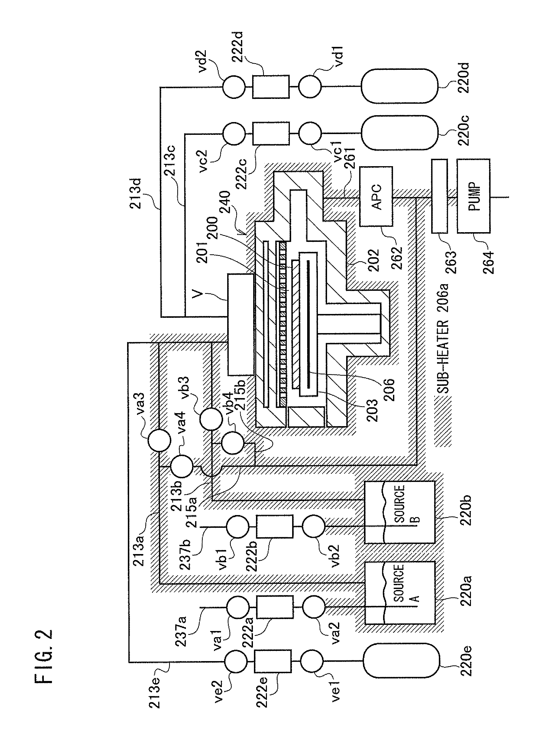
[0101]Further, according to this embodiment, formation of the first metal film (TiN film) by CVD method and formation of the second metal film (AlN film) by ALD method are not simultaneously performed, but performed separately. Moreover, in the CVD-TiN step (S6), the purging step is performed after the first source gas supplying step, to thereby surely perform gas replacement in the processing chamber 201. Further, in the ALD-AlN step (S8) also, purging is performed lastly in a cycle process, and the gas in the processing chamber 201 is surely replaced. Thus, the first source gas and the second source gas are not mixed with each other in the processing chamber 201, and it is possible to suppress the generation of particles due to vapor phase reaction between the first source gas and the second source gas in the processing chamber 201, and improve uniformity in film thickness and composition of the metal composite film (TiAlN film). Note the if the formation of the first metal film (TiN film) by CVD method and the formation of the second metal film (AlN film) by ALD method are simultaneously performed, mixing time and reaction of the first source gas and the second source gas need to be considered, thus making it difficult to control the film thickness and the composition. Further, particles are generated due to vapor phase reaction between the first source gas and the second source gas, resulting in deterioration in the film thickness and the composition of the metal composite film (TiAlN film) in some cases, depending on the combination of gas species.
[0102]Also, according to this embodiment, a relatively high temperature process is used in forming the first metal film (TIN film) by CVD method. Therefore, an ALD precursor having relatively high decomposition temperature is selected in forming the second metal film (AlN film). Namely, CVD / ALD is executed at high temperature, and therefore residual impurities in the film can be lessened by heat, without using a damage source such as plasma (non-plasma).
[0103]Further, according to this embodiment, use amount of the precursor can be lessened, compared with that of a related art wherein film formation is performed only by ALD method, and therefore it is advantageous in terms of cost.
[0104]The aforementioned embodiment describes an example of vaporizing the liquid source contained inside of the bubbler by bubbling. However, the liquid source may be vaporized by using a vaporizer instead of the bubbler.

Problems solved by technology

However, when the metal composite film is formed by ALD method, there is a problem that residual impurities resulting from the precursor can not be completely removed, due to its low processing temperature.
Meanwhile, the metal composite film is also formed by PEALD method using plasma as shown in the non-patent document 1, However, when a film is formed by PALD method, flatness of the film is sometimes deteriorated, and when this method is applied to formation of the gate electrode, because plasma is used, there is a risk of plasma damage added to a gate insulating film and increase of EOT.
Also, when the metal composite film is formed by ALD method by alternate supply of two kinds of precursors and reactive gas, its film-forming rate is problematic, thus involving a great problem that tremendous time is required and the precursor is wasted.

Method used


Image

  • Method of manufacturing semiconductor device and substrate processing apparatus
  • Method of manufacturing semiconductor device and substrate processing apparatus
  • Method of manufacturing semiconductor device and substrate processing apparatus

Examples


example 1

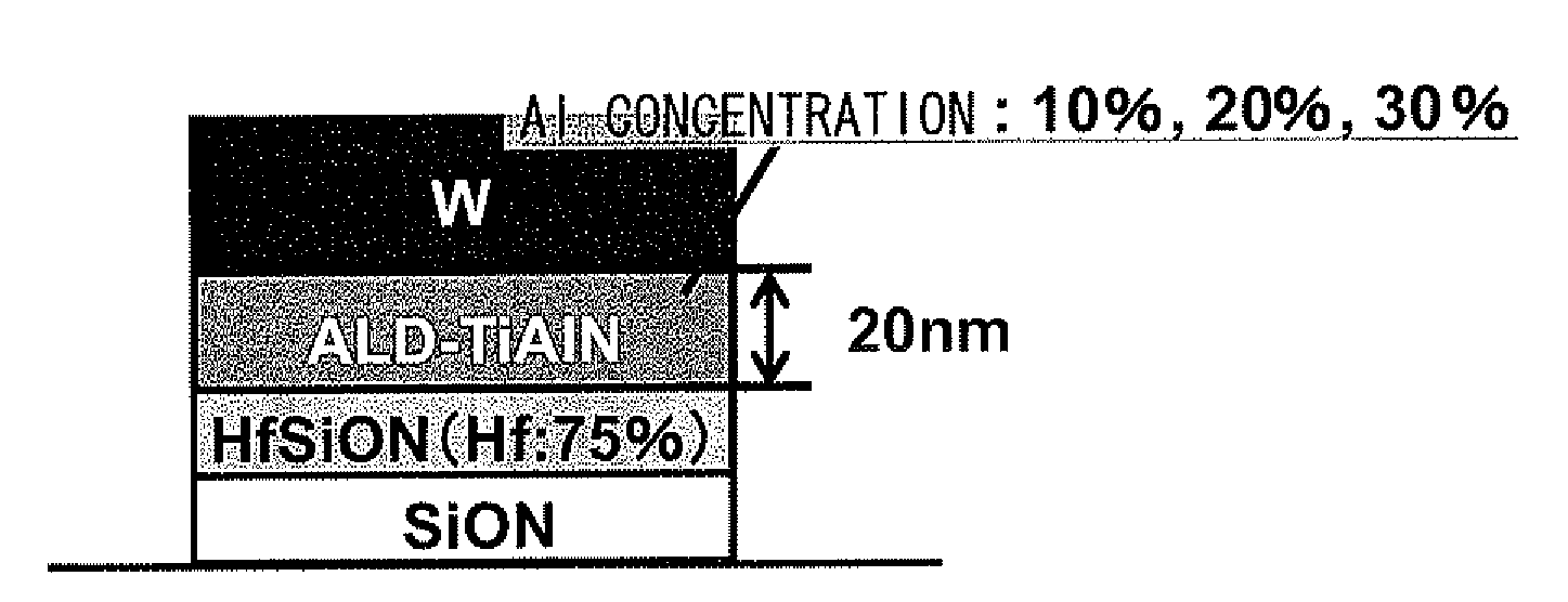
[0108]As an example 1 of the present invention, evaluation of the film formation rate of the CVD-TiN film formation and the ALD-AlN film formation will be described. FIG. 6A is a view showing TDMAT supply time dependency of the CVD-TiN film thickness on the HfSiON, AlN, SiO2 in the CVD-TiN film formation. FIG. 6A shows the TDMAT supply time taken on the horizontal axis and the TiN film thickness taken on the vertical axis. FIG. 5B is a view showing the ALD cycle number dependency of the ALD-AlN film thickness on the HfSiON, TiN, SiO2 in the ALD-AlN film formation. FIG. 6B shows the number of cycles of ALD-AlN taken on the horizontal axis, and the AlN film thickness taken on the vertical axis. Note that the CVD-TiN film formation and the ALD-AlN film formation in this evaluation are performed, with the processing conditions set in the values within the processing conditions in the aforementioned embodiments.

[0109]It is found from FIG. 6A, that almost no change occurs in the film form...

example 2

[0111]As an example 2 of the present invention, explanation will be given for a film formation evaluation (analysis by sectional TEM photograph) of a laminate film, by repeating the CVD-TiN film formation and the ALD-AlN film formation. FIG. 7A shows the sectional TEM photograph after repeating the ALD-AlN film formation and the CVD-TiN film formation and forming the laminate film composed of 5-layers (TiAlN of 5-layers), laminate film composed of 11-layers (TiAlN of 11-layers), and laminate film composed of 21-layers (TiAlN of 21-layers) respectively. Also, FIG. 7B shows the sectional TEM photograph after repeating the ALD-AlN film formation and the CVD-TiN film formation and forming the laminate film composed of 5-layers (TiAlN of 5-layers), laminate film composed of 11-layers (TiAlN of 11-layers), and laminate film composed of 21-layers (TiAlN of 21-layers) respectively, with N2 annealing applied thereto at 900° C. Note that either of the CVD-TiN film formation and the ALD-AlN fi...

example 3

[0113]As an example 3 of the present invention, explanation will be given for a film formation evaluation (profile analysis in XPS depth direction) of the laminate film by repeating the CVD-TiN film formation and the ALD-AlN film formation. FIG. 8A is a view showing a profile in the XPS depth direction after the laminate film composed of 11-layers (22 nm) (TiAlN of 11-layers) is formed (TiN:2 nm, AlN:2 nm) and N2 annealing is applied thereto at 900° C., and FIG. 8B is a view showing the profile in the XPS depth direction after the laminate film composed of 21-layers (21 m) (TiAlN of 21-layers) is formed (TiN:1 nm, AlN:1 nm) and annealing is applied thereto at 900° C. Each view shows a sputtering time (same as the depth direction) taken on the horizontal axis, and the concentration of each atom in the film taken on the vertical axis. Note that the CVD-TiN film formation and the ALD-AlN film formation in this evaluation was performed, with the processing conditions set to be the value...


PUM

PropertyMeasurementUnit
temperatureaaaaaaaaaa

Abstract

A manufacturing method of a semiconductor device of the present invention includes the step of forming an insulating film on a substrate, and the step of forming a high dielectric constant insulating film on the insulating film, and the step of forming a titanium aluminium nitride film on the high dielectric constant insulating film, wherein in the step of forming the titanium aluminum nitride film, formation of an aluminium nitride film and formation of a titanium nitride film are alternately repeated, and at that time, the aluminium nitride film is formed firstly and / or lastly.

Description

BACKGROUND[0001]1. Technical Field[0002]The present invention relates to a manufacturing method of a semiconductor device and a substrate processing apparatus, and particularly relates to the manufacturing method of the semiconductor device including the step of forming a metal film on a substrate and the substrate processing apparatus for forming the metal film on the substrate.[0003]2. Description of Related Art[0004]In a Metal / High-k gate stack, when high-temperature heat treatment is applied, there is a problem that an effective work function of a metal gate electrode is shifted to midgap, due to Fermi-level pinning phenomenon. This phenomenon appears remarkably in p-MOSFET in particular. As a method of avoiding this phenomenon, research of using a metal composite film, such as a Metal-Al—N film, in the gate electrode, has been recently conducted. A TiAlN film and a RuAlN film are given as examples of the Metal-Al—N film.[0005]As a conventional film-forming method of the metal c...

Claims


Application Information

Patent Timeline
Patent Type & Authority Applications(United States)
IPC IPC(8): H01L21/28B05C11/00
CPCC23C16/34C23C16/45523C23C16/45531H01L29/517H01L29/495H01L29/513H01L21/28088H01L21/31
Inventor HARADA, KAZUHIRO
Owner KOKUSA ELECTRIC CO LTD
Learn More