Memory device with power noise minimization during sensing

a memory device and power noise technology, applied in the field of nonvolatile memory, can solve the problems of various errors in the sensing process, and achieve the effect of reducing the effect of power noise in the sense amplifier supply and increasing accuracy

Active Publication Date: 2009-12-31
SANDISK TECH LLC
View PDF0 Cites 11 Cited by
  • Summary
  • Abstract
  • Description
  • Claims
  • Application Information

AI Technical Summary

Benefits of technology

[0012]The present invention relates to a memory device in which storage elements are sens

Problems solved by technology

However, the sensing process is

Method used


Image

  • Memory device with power noise minimization during sensing
  • Memory device with power noise minimization during sensing
  • Memory device with power noise minimization during sensing

Examples


Embodiment Construction

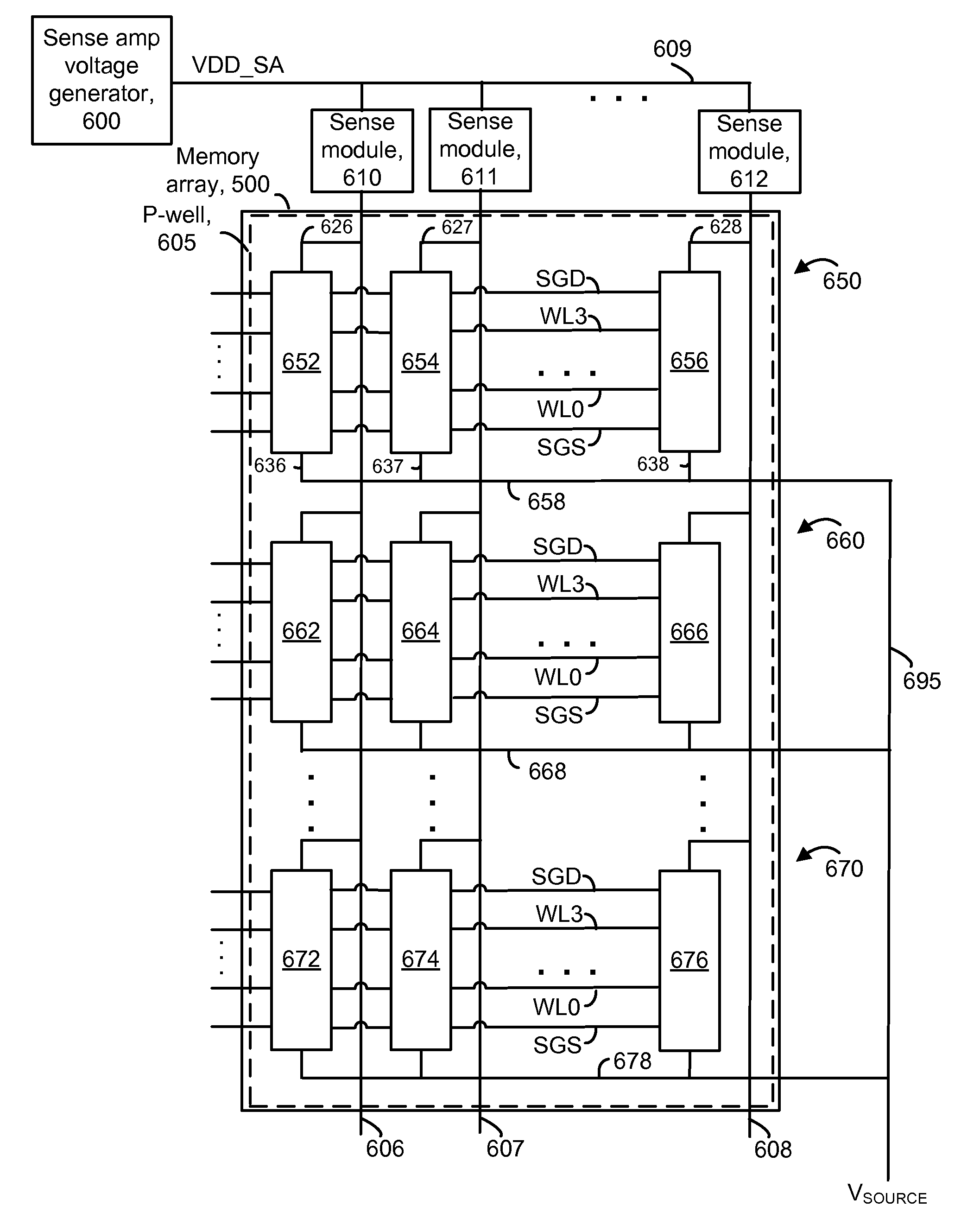
[0030]The present invention relates to a memory device in which storage elements are sensed with increased accuracy by reducing the effects of sense amplifier supply power noise.

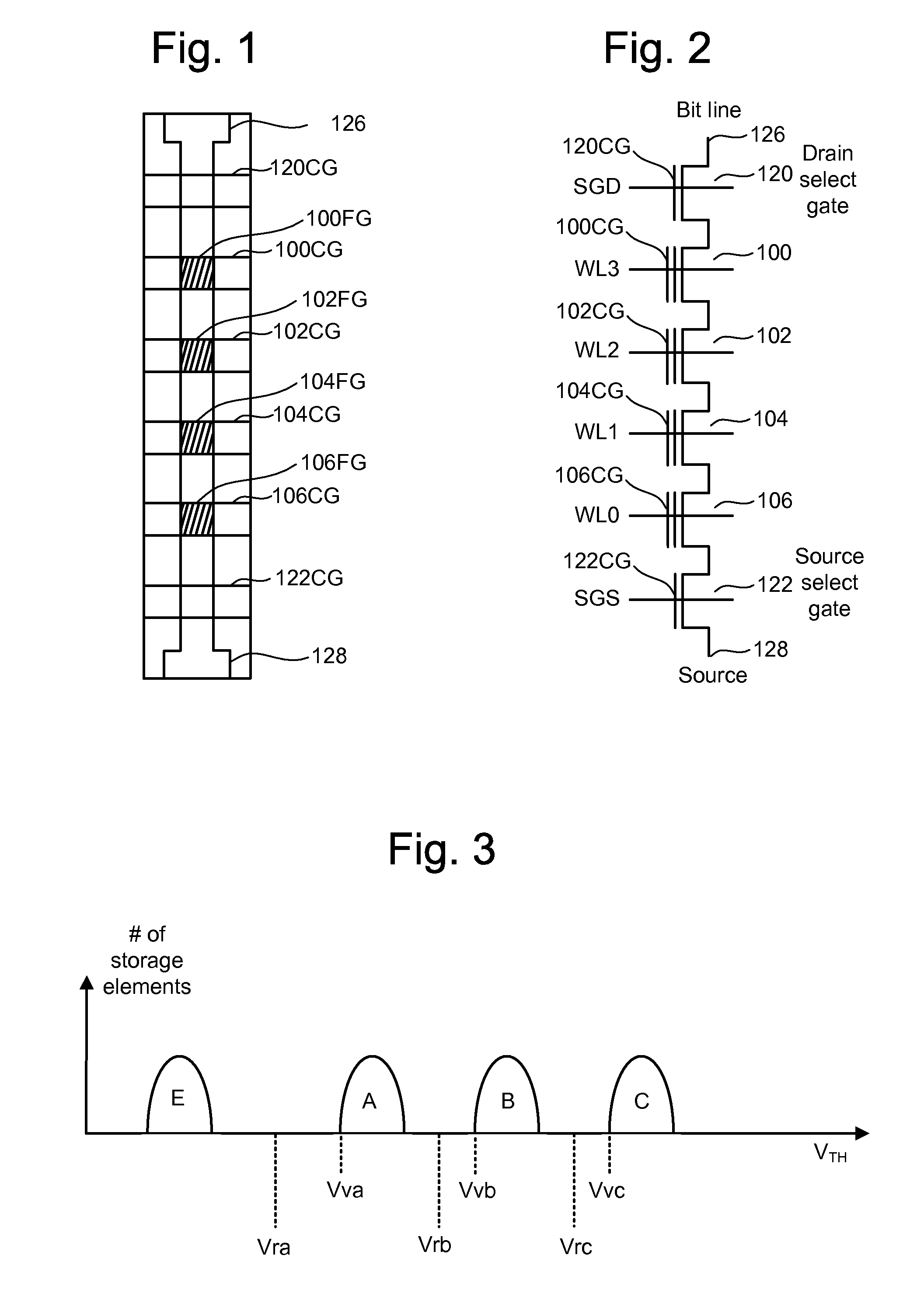
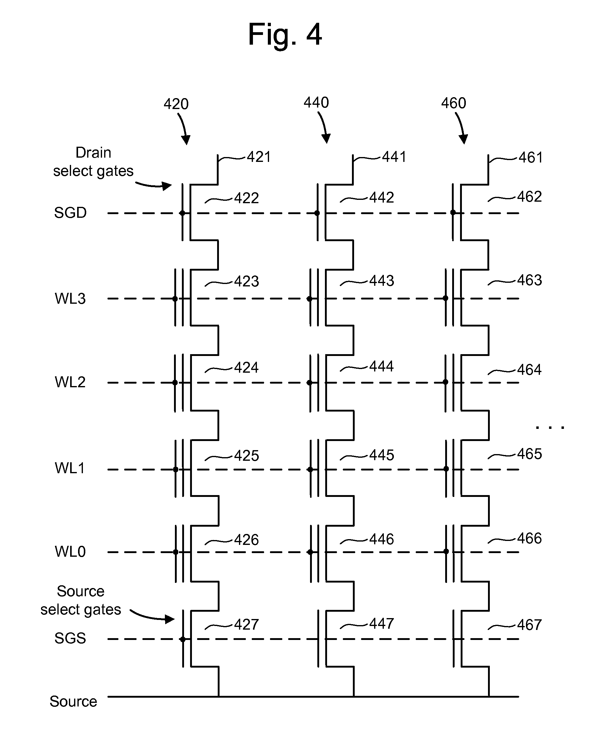
[0031]One example of a memory system suitable for implementing the present invention uses the NAND flash memory structure, which includes arranging multiple transistors in series between two select gates. The transistors in series and the select gates are referred to as a NAND string. FIG. 1 is a top view showing one NAND string. FIG. 2 is an equivalent circuit thereof. The NAND string depicted in FIGS. 1 and 2 includes four transistors, 100, 102, 104 and 106, in series and sandwiched between a first select gate 120 and a second select gate 122. Select gate 120 gates the NAND string connection to bit line 126. Select gate 122 gates the NAND string connection to source line 128. Select gate 120 is controlled by applying the appropriate voltages to control gate 120CG. Select gate 122 is controlled by applying ...


PUM


Abstract

Accuracy of sensing operations, such as read or verify, in a memory device is improved by avoiding fluctuations in a sense amp supply voltage which can occur when different sense amps are strobed at different times. First and second sets of sense amps perform a sensing operation on respective storage elements, such as in an all bit line configuration. The first set of sense amps is strobed at a first time point. In response, a sensed analog level is converted to digital data. The A/D conversion relies on the sense amp supply voltage being accurate. To avoid a fluctuation in the sense amp supply voltage, a bypass path allows the storage elements associated with the first set of sense amps to continue to draw power from the sense amp supply voltage. The second set of sense amps is strobed at a later, second time point.

Description

CROSS-REFERENCE TO RELATED APPLICATIONS[0001]This application is related to co-pending, commonly-assigned U.S. patent application ______ , titled “Minimizing Power Noise During Sensing In Memory Device”, attorney docket no. SAND-01337US0, filed herewith, and incorporated herein by reference.BACKGROUND OF THE INVENTION[0002]1. Field of the Invention[0003]The present invention relates to non-volatile memory.[0004]2. Description of the Related Art[0005]Semiconductor memory has become increasingly popular for use in various electronic devices. For example, non-volatile semiconductor memory is used in cellular telephones, digital cameras, personal digital assistants, mobile computing devices, non-mobile computing devices and other devices. Electrically Erasable Programmable Read Only Memory (EEPROM) and flash memory are among the most popular non-volatile semiconductor memories. With flash memory, also a type of EEPROM, the contents of the whole memory array, or of a portion of the memor...

Claims


Application Information

Patent Timeline
IPC IPC(8): G11C16/06G11C5/14
CPCG11C5/147G11C16/26G11C16/0483
Inventor LEE, SEUNGPILNGUYEN, HAO THAIMUI, MAN LUNG
Owner SANDISK TECH LLC
Why Eureka
Try Eureka