
Nano-fabricated superconducting radio-frequency composites, method for producing nano-fabricated superconducting RF composites

Active Publication Date: 2009-12-17
UCHICAGO ARGONNE LLC
View PDF2 Cites 10 Cited by
  • Summary
  • Abstract
  • Description
  • Claims
  • Application Information

AI Technical Summary

Benefits of technology

[0016]A further object of the present invention is to provide a method for producing accelerator superconducting cavities with gradients as high as 100 MV / m. A feature of the invention is the serial application of one or several materials on an underlying substrate, whereby each of the layers is uniformly one molecule or atom thick. An advantage of the invention is the elimination of the elaborate cleaning and etching processes currently required when producing rf cavity surfaces. Another advantage of this invention is its use in situ, (i.e., when the cavity is already incorporated in an accelerator) so as to avoid contamination, and / or as part of ongoing maintenance.
[0017]Another object of the present invention is to provide superconducting accelerator cavities which are 50 percent shorter than typical structures producing similar acceleration. A feature of the invention covering a superconducting underlayment with layers of insulating material arranged in alternating configurations with layers of superconducting material. An advantage of the invention is that the insulating materials shield the superconducting underlayment from quenching magnetic fields while simultaneously directing oxygen from the original surface of the underlayment and into the bulk of the underlayment.
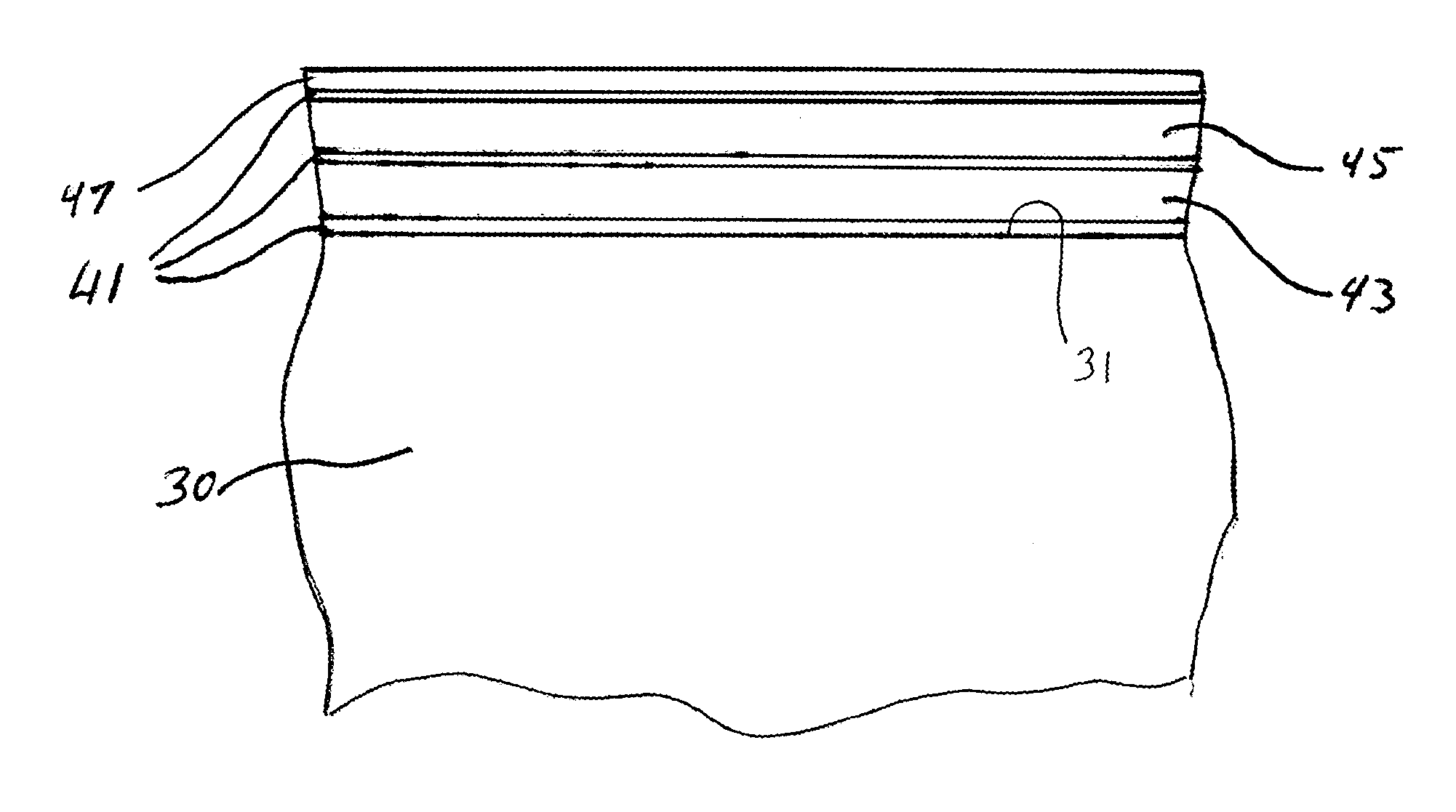
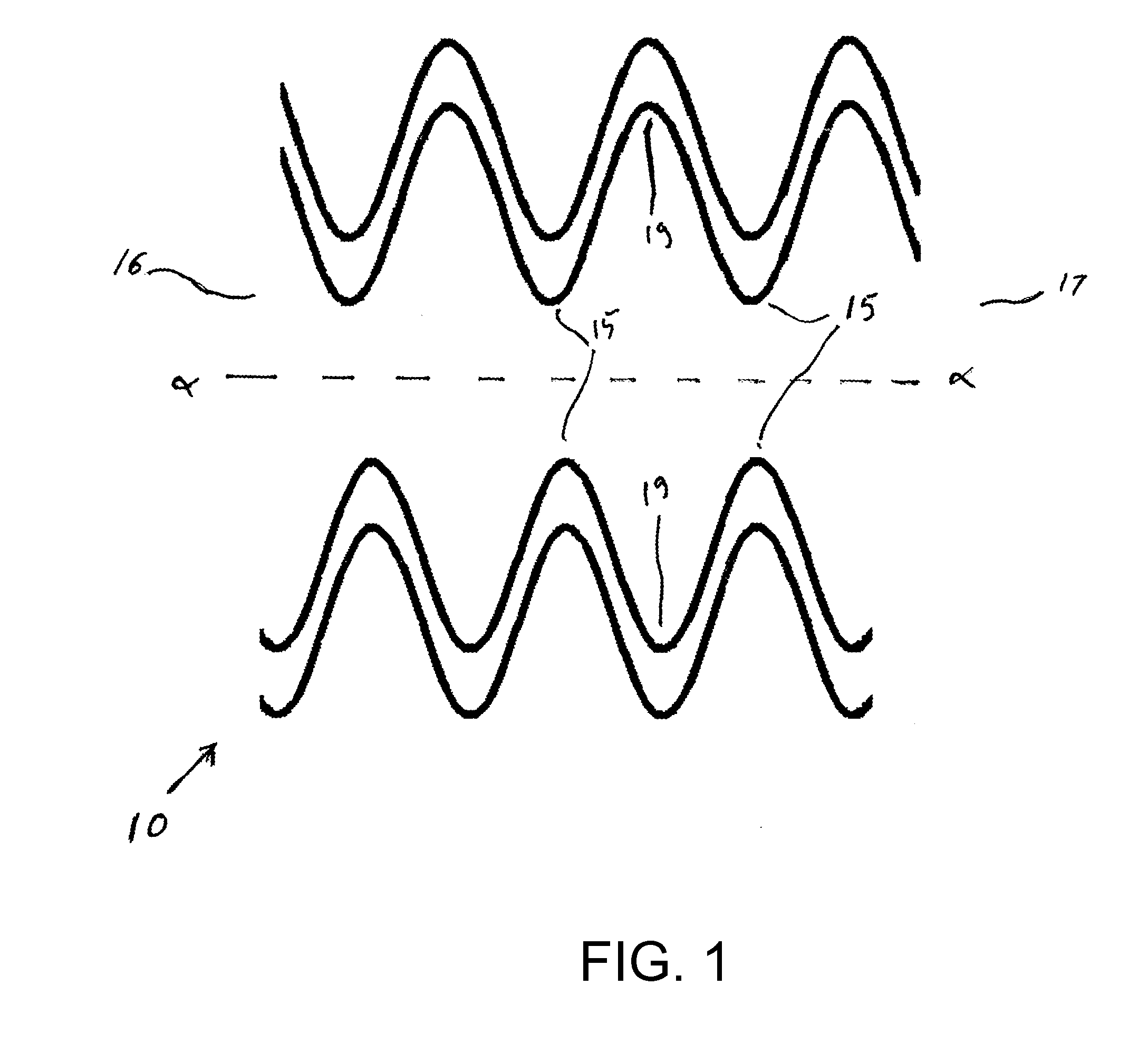
[0018]Briefly, the invention provides a radio-frequency accelerator cavity adapted to accommodate an accelerating voltage gradient between 30 MV / m and 100 MV / m, the cavity comprising a superconducting substrate defining a conduit; a dielectric layer covering interior surfaces of the conduit; a first superconducting layer covering said dielectric layer; and succeeding alternating dielectric and superconducting layers overlaying said first superconducting layer.
[0019]Also provided is a radio-frequency accelerator cavity adapted to accommodate an accelerating voltage gradient between 30 MV / m and 100 MV / m, the cavity comprising a superconducting substrate defining a conduit; a dielectric layer covering interior surfaces of the conduit; and a superconducting layer covering said dielectric layer.
[0020]The invention also provides a method for producing a superconducting radio-frequency accelerator cavity having a surface accelerating voltage gradient between 30 MV / m and 100 MV / m, the method comprising coating inner walls of the cavity with one or more materials with each of said materials deposited in one or more layers that are one atom thick. One or more of said materials may be chosen to be a superconductor and one or more of said materials may be chosen to be a dielectric.
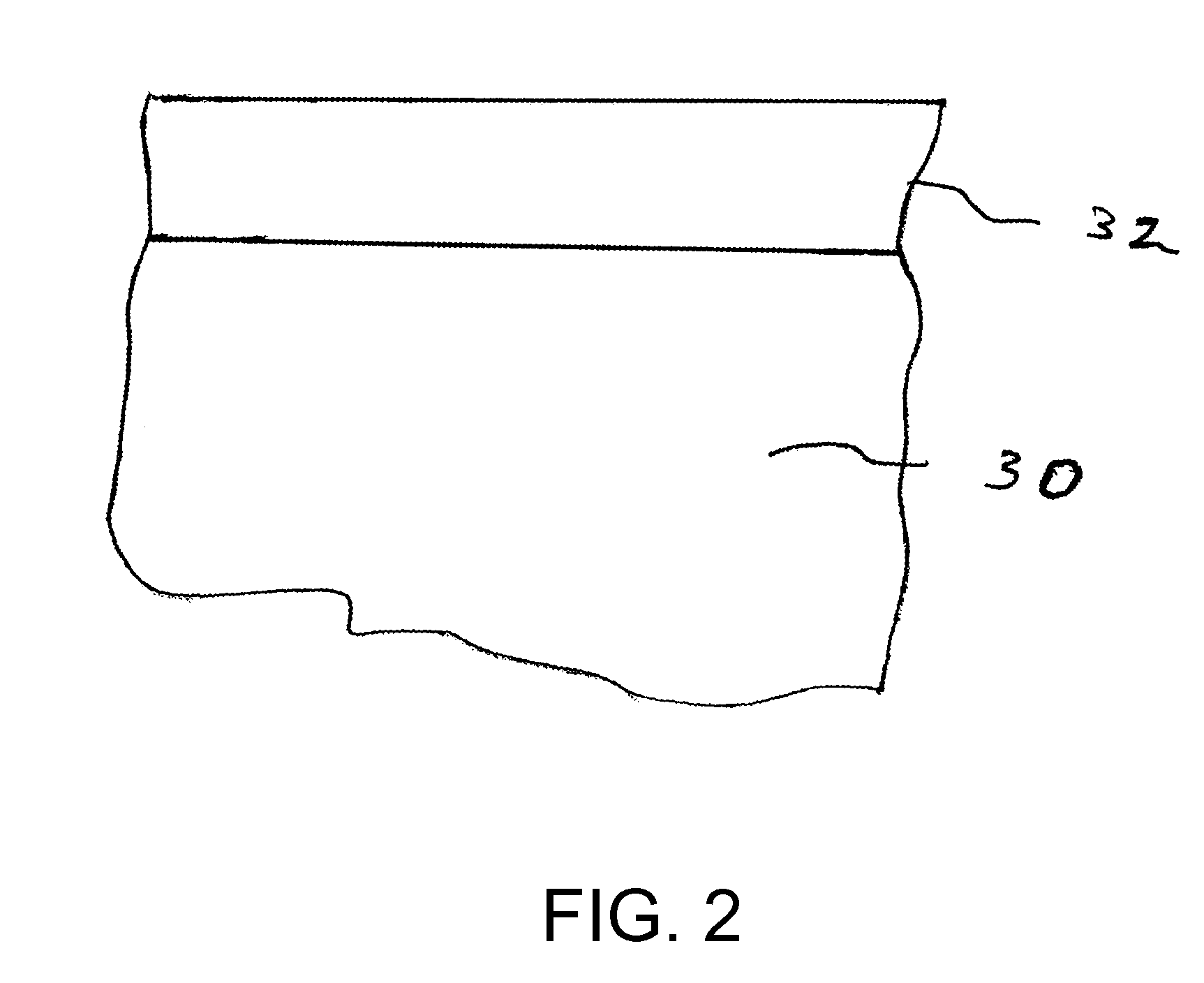
[0021]The invention further provides a method for producing a radio-frequency accelerator cavity having a surface accelerating voltage gradient between 30 MV / m and 100 MV / m, said method comprising subjecting a superconducting substrate to a controlled atmosphere; coating the substrate with a dielectric so as to form a first layer on the substrate; and coating the first layer with a superconductor so as to form a surface having a root mean square roughness of less than 0.4 nanometer.

Problems solved by technology

Superconducting radio-frequency (“SCRF”) cavities have been adopted throughout the world for the acceleration of particle beams, but SCRF cavities have not been able to routinely reach theoretically expected performance for a variety of reasons.
As a result, accelerator designs have been increasing in complexity, cost, and length over the past decades, due to the inability to increase the accelerating voltage gradient of superconducting cavities over 30 MV / m (Million Volts / meter).
As the regenerated current is confined within roughly the first 100 nanometers of the cavity's surface, the main sources of cavity failure are these surface imperfections.
Cavities fabricated from ordinary metals, such as copper, silver, stainless steel, can also fail at comparable gradients.

Method used


Image

  • Nano-fabricated superconducting radio-frequency composites, method for producing nano-fabricated superconducting RF composites
  • Nano-fabricated superconducting radio-frequency composites, method for producing nano-fabricated superconducting RF composites
  • Nano-fabricated superconducting radio-frequency composites, method for producing nano-fabricated superconducting RF composites

Examples


example

[0079]An embodiment of the present invention is a coating layer of alumina, Al2O3, several molecules thick to cover a niobium surface with a chemically impermeable insulator. Next a layer of niobium fluoride is deposited on the alumina surface, and then another layer of alumina is deposited to protect the niobium from oxidation. Alumina is a good thermal conductor, a good electrical conductor, and resists oxidation. The first layer of alumina will permit any oxygen attached to the niobium substrate to migrate into the interior of the substrate and mitigate any decline in material properties. The surface with a combination of alumina / niobium fluoride / alumina on bulk niobium enables the resulting construct to operate at significantly higher fields than have been seen in any existing rf structure.

[0080]Other materials, such as magnesium diboride as a superconducting layer, and additional layers of alumina, are added to provide different properties. The inventors found that vortexes, wh...


PUM

PropertyMeasurementUnit
Temperatureaaaaaaaaaa
Timeaaaaaaaaaa

Abstract

Superconducting rf is limited by a wide range of failure mechanisms inherent in the typical manufacture methods. This invention provides a method for fabricating superconducting rf structures comprising coating the structures with single atomic-layer thick films of alternating chemical composition. Also provided is a cavity defining the invented laminate structure.

Description

[0001]This utility application claims the benefits of U.S. Provisional Application No. 60 / 998,619 filed on Oct. 12, 2007.CONTRACTUAL ORIGIN OF THE INVENTION[0002]The United States Government has rights in this invention pursuant to contract number DE-AC02-06CH11357 between the U.S. Department of Energy and the University of Chicago representing Argonne National Laboratory.BACKGROUND OF THE INVENTION[0003]1. Field of the Invention[0004]This invention relates to an improved method for preparing radio-frequency (“rf”) accelerator cavities, and more particularly, this invention relates to an improved method for preparing high voltage-gradient superconducting rf cavities through controlled deposition of dielectric and superconducting materials.[0005]2. Background of the Invention[0006]Superconductors are metals that exhibit vanishing resistance at very low temperatures, i.e. temperatures a few degrees above absolute zero (0 degrees Kelvin). Typically, such temperatures are achieved by pl...

Claims


Application Information

Patent Timeline
IPC IPC(8): H01P1/203H01L39/24
CPCH01J23/20H01L39/24H01L39/14H10N60/20H10N60/01
Inventor NOREM, JAMES H.PELLIN, MICHAEL J.
Owner UCHICAGO ARGONNE LLC
Learn More