
Apparatus and system for a single element solar cell

a solar cell and apparatus technology, applied in the field of solar cell devices, can solve the problems of increasing complexity and cost, limited useful power conversion in the optical frequency range, and generally considered low conversion efficiency of solar cells

Inactive Publication Date: 2009-12-17
SCITECH ASSOCS HLDG
View PDF4 Cites 52 Cited by
  • Summary
  • Abstract
  • Description
  • Claims
  • Application Information

AI Technical Summary

Benefits of technology

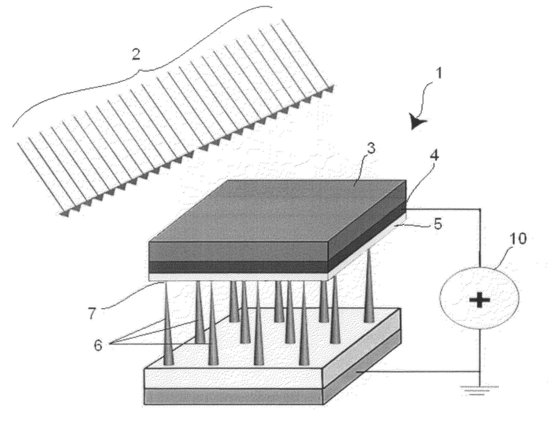
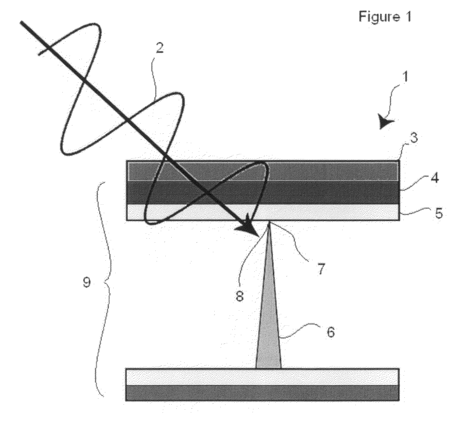
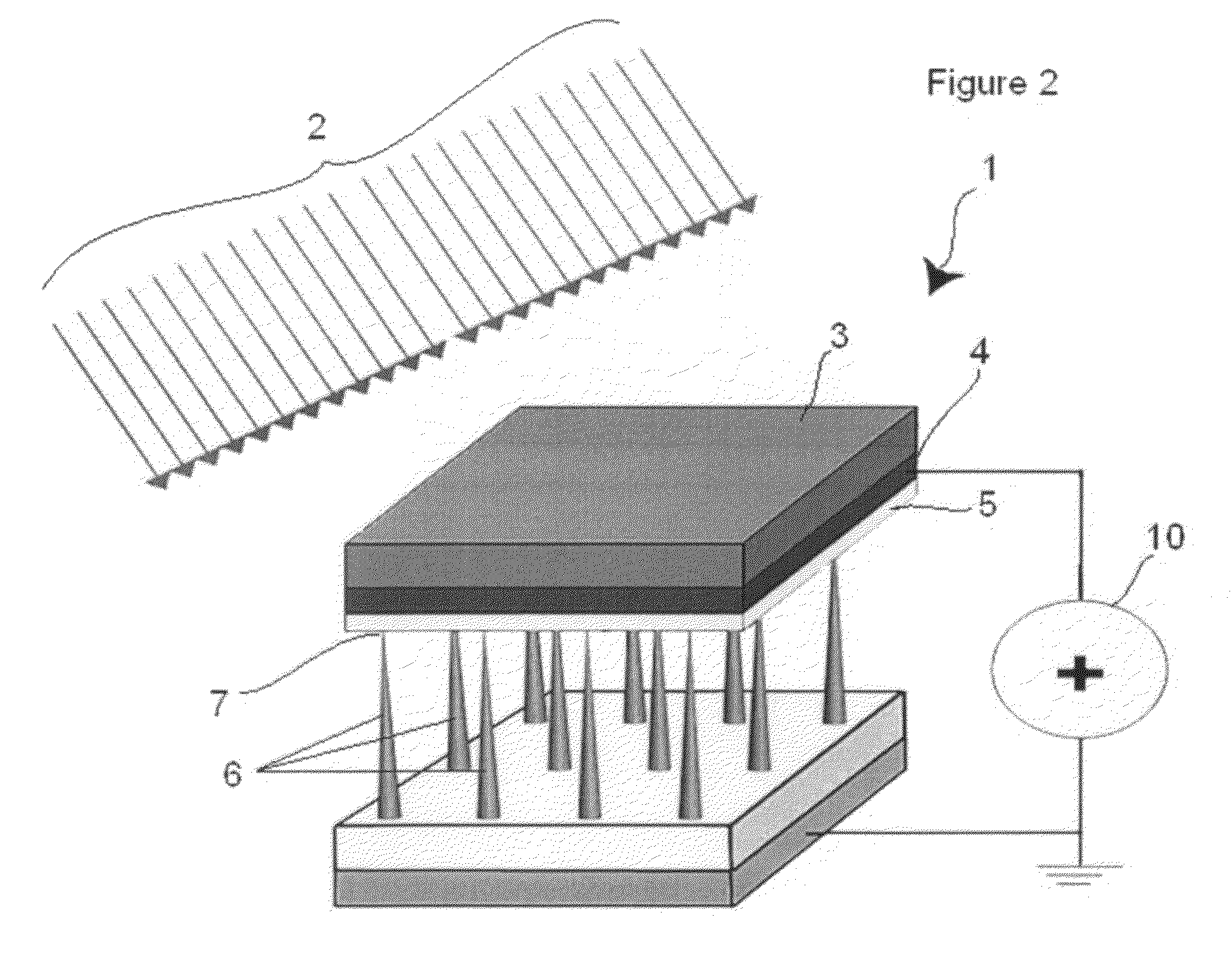
"The present invention is a device that uses a single element rectenna made from metallic carbon nanotubes or nanowires to capture and convert incident radiation into useful electrical energy. The nanowires / mCNTs act as both a receiving antenna and a rectifying diode, providing asymmetric tunneling barriers that allow for asymmetric tunneling currents. The device has a high sensitivity to incident radiation and can capture more energy than standard solar cells. The nanowires / mCNTs have a sharp edge and may be made of metals such as tungsten, molybdenum, nickel, gold, or silver. The device may be used in conjunction with an external load to store the captured energy."

Problems solved by technology

However, these solar cells are generally considered to have relatively low conversion efficiencies.
While it may be possible to increase the maximum obtainable efficiency by using multi-junction solar cells, this requires increased complexity and cost.
It is believed, however, that useful power conversion in the optical frequency range may be limited by the low frequency response of the planar diodes employed in the foregoing studies (in particular, the diodes were 100 nanometer square in the ITN device).
Prior efforts to develop solar cells using standard two-element rectennas are believed to have had limited success due to the frequency limited response of the planar MIM diodes.

Method used


Image

  • Apparatus and system for a single element solar cell
  • Apparatus and system for a single element solar cell
  • Apparatus and system for a single element solar cell

Examples


Embodiment Construction

[0043]In the solar cell apparatus and system of the present invention, the problem of the low frequency response of the planar MIM diodes is intended to be overcome by using the individual constituents of a vertical array of aligned metallic carbon nanotubes (mCNTs) and / or nanowires (which may be metallic tips or whiskers), where each one acts as a combined antenna and rectifier in a point-contact configuration. With the present system, point-contact devices (which have been used in measurements of absolute frequencies of lasers up to the green part of the visible spectrum and which demonstrate a response time of the order of femotseconds that is significantly faster than standard MIM diodes, and which are not believed to have been previously used in solar cells) are used in the exemplary embodiments of the present invention, as described herein.

[0044]As shown in FIG. 1, the solar cell 1 receives incident solar radiation 2 through a transparent cover layer 3. The transparent cover l...


PUM


Abstract

A device for receiving and converting incident radiation into DC current, the device including a transparent conductor, at least one point-contact diode, the at least one point-contact diode having a nanowire / mCNT providing a receiving antenna function and a rectification function, a thin insulating layer situated between the transparent conductor and the nanowire / mCNT, and a point contact junction at which the nanowire / mCNT contacts the thin insulating layer.

Description

FIELD OF THE INVENTION[0001]The present invention relates to a solar cell device for receiving and converting incident radiation into DC current.BACKGROUND INFORMATION[0002]Solar energy is an abundant renewable energy source. It has been estimated that the sun deposits more than 12,000 terrawatts (TW) of energy on Earth, which is large compared to the 13 TW of total current power consumption worldwide. Thus, converting even 0.1% of the sunlight into useful electricity could eventually meet the total current power consumption worldwide.[0003]There are various ways to capture, store and convert solar radiation in useful forms of energy. Solar cells are one way to directly convert sunlight into electricity. Various materials and technologies have been developed that involve single crystal, polycrystalline, amorphous and nanostructured inorganic and organic materials for use in solar cells. More recently, multi-junction cells, quantum dots and dye sensitized photovoltaics have received ...

Claims


Application Information

Patent Timeline
Patent Type & Authority Applications(United States)
IPC IPC(8): H01L31/00
CPCB82Y10/00H01L27/301Y02E10/549H01L51/0048H01L51/42H01L31/03529H01L31/035227H01L31/1085H10K85/221H10K39/10H10K30/00
Inventor CUTLER, PAUL H.
Owner SCITECH ASSOCS HLDG
Learn More