Method for fabricating multilayered encapsulation thin film having optical functionality and mutilayered encapsulation thin film fabricated by the same
a technology of multi-layer encapsulation and muti-layer encapsulation, which is applied in the direction of vacuum evaporation coating, transportation and packaging, coatings, etc., can solve the problems of power reduction and/or early deterioration of the device performance, the general structure of the electronic display device such as the organic light emitting device (“oled”) or the liquid crystal display (“lcd”) is easily damaged by oxygen or moisture, and the metal substance generally has limited transparency
- Summary
- Abstract
- Description
- Claims
- Application Information
AI Technical Summary
Benefits of technology
Problems solved by technology
Method used
Image
Examples
example 1
Fabrication of Multilayered Encapsulation Thin Film
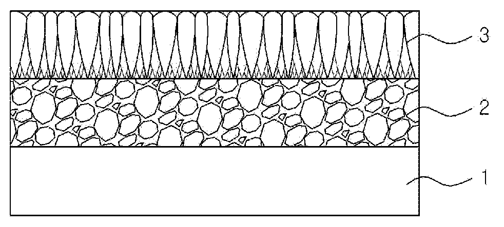
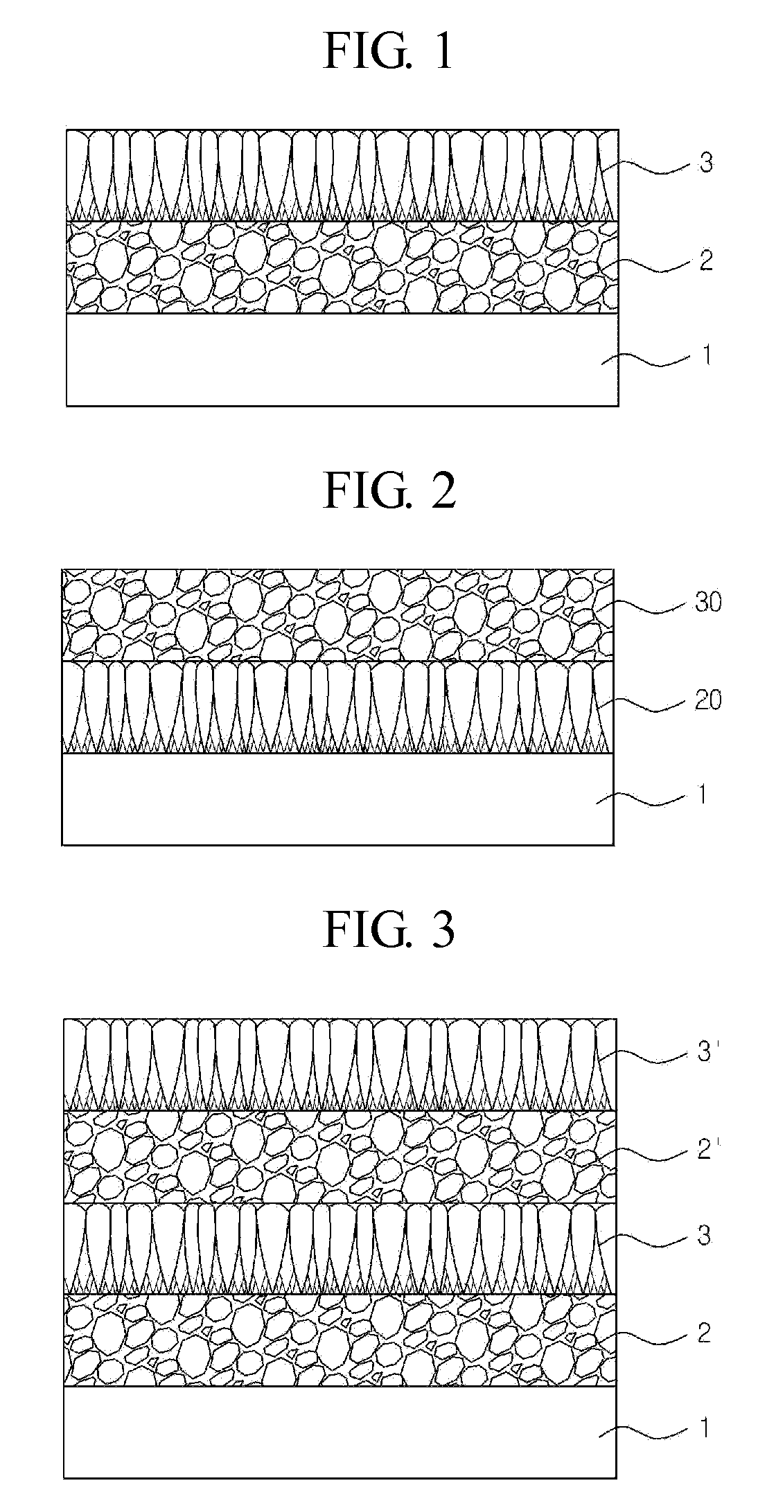
[0079]Using a physical vapor deposition system Sputter Infovion No. 3 available from Infovion Co., Ltd. (2 gun co-sputtering, 6 inch substrate), a first thin film is formed on a polyethylene terephthalate (“PET”) substrate with a thickness of 100 μm. Some targets contained in a vacuum chamber of the system are used to form the first thin film by a reactive RF magnetron sputtering process. The used targets are Al (Ø6″, 99.99% purity). After Ar (98 sccm) and O2 (2 sccm) are fed to the vacuum chamber to separate Al from the targets, an electric field is applied to the Al targets, to proceed with a reaction of the separated Al with O2. As a result, an Al2O3 thin film (first thin film) is formed on the substrate. The sputtering is continued for 1,200 seconds.
[0080]Next, the remaining targets are used to form a second thin film by a non-reactive RF magnetron sputtering process. The used targets are Al2O3 (Ø6″, 99.99% purity). First, after...
example 2
Fabrication of Multilayered Encapsulation Thin Film
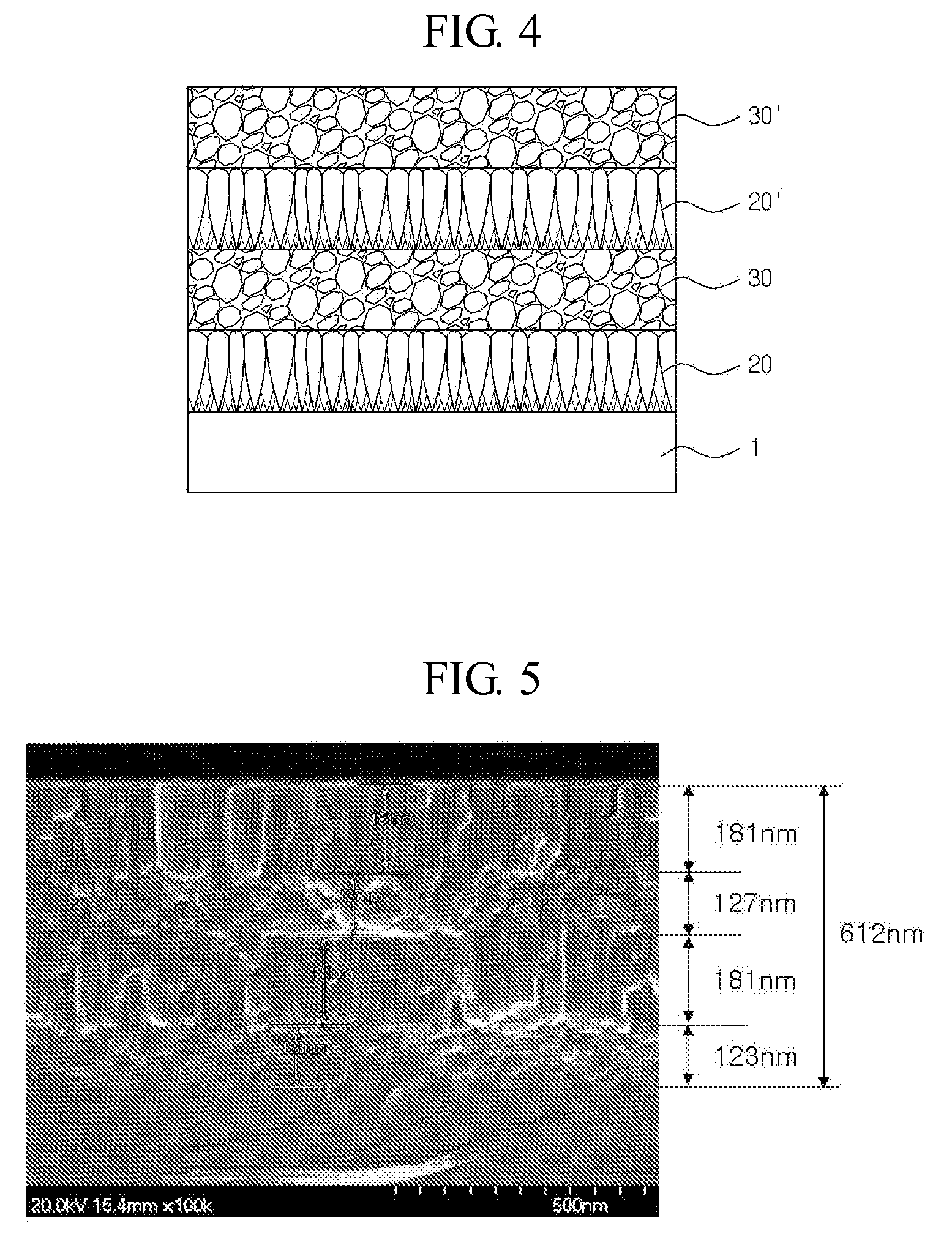
[0081]A multilayered encapsulation thin film is fabricated according to the same procedure as in Example 1, except that the process including formation of the first thin film followed by formation of the second film is repeated twice. FIG. 5 shows a cross-sectional field electron scanning electron microscope (“FE-SEM”) photograph of the resultant multilayered encapsulation thin film. Referring to FIG. 5, it may be seen that this thin film included four layers including a first thin film (123 nm), a second thin film (181 nm), another first thin film (127 nm) and another second thin film (181 nm) laminated on a substrate in this order. The multilayered encapsulation thin film has a thickness of 612 nm.
example 3
Fabrication of Multilayered Encapsulation Thin Film
[0082]A multilayered encapsulation thin film is fabricated according to the same procedure as in Example 1, except that the first thin film is firstly formed by a non-reactive RF magnetron sputtering process, followed by formation of the second thin film using a reactive RF magnetron sputtering process.
PUM
| Property | Measurement | Unit |
|---|---|---|
| optical functionality | aaaaa | aaaaa |
| density | aaaaa | aaaaa |
| refractive index | aaaaa | aaaaa |
Abstract
Description
Claims
Application Information
 - R&D
- Intellectual Property
- Life Sciences
- Materials
- Tech Scout
- Unparalleled Data Quality
- Higher Quality Content
- 60% Fewer Hallucinations
Browse by: Latest US Patents, China's latest patents, Technical Efficacy Thesaurus, Application Domain, Technology Topic, Popular Technical Reports.
© 2025 PatSnap. All rights reserved.Legal|Privacy policy|Modern Slavery Act Transparency Statement|Sitemap|About US| Contact US: help@patsnap.com


