Thin film solar cells with monolithic integration and backside contact
a solar cell and monolithic technology, applied in the field of thin film solar cells, can solve the problems of film solar cells, limited current generated by film solar cells/modules, and heavy cdte solar cells,
- Summary
- Abstract
- Description
- Claims
- Application Information
AI Technical Summary
Benefits of technology
Problems solved by technology
Method used
Image

Examples
example 1
A Thin-Film CdTe Solar Cell on a Flexible Insulating Substrate with Serial Interconnects and a Back Metal Contact
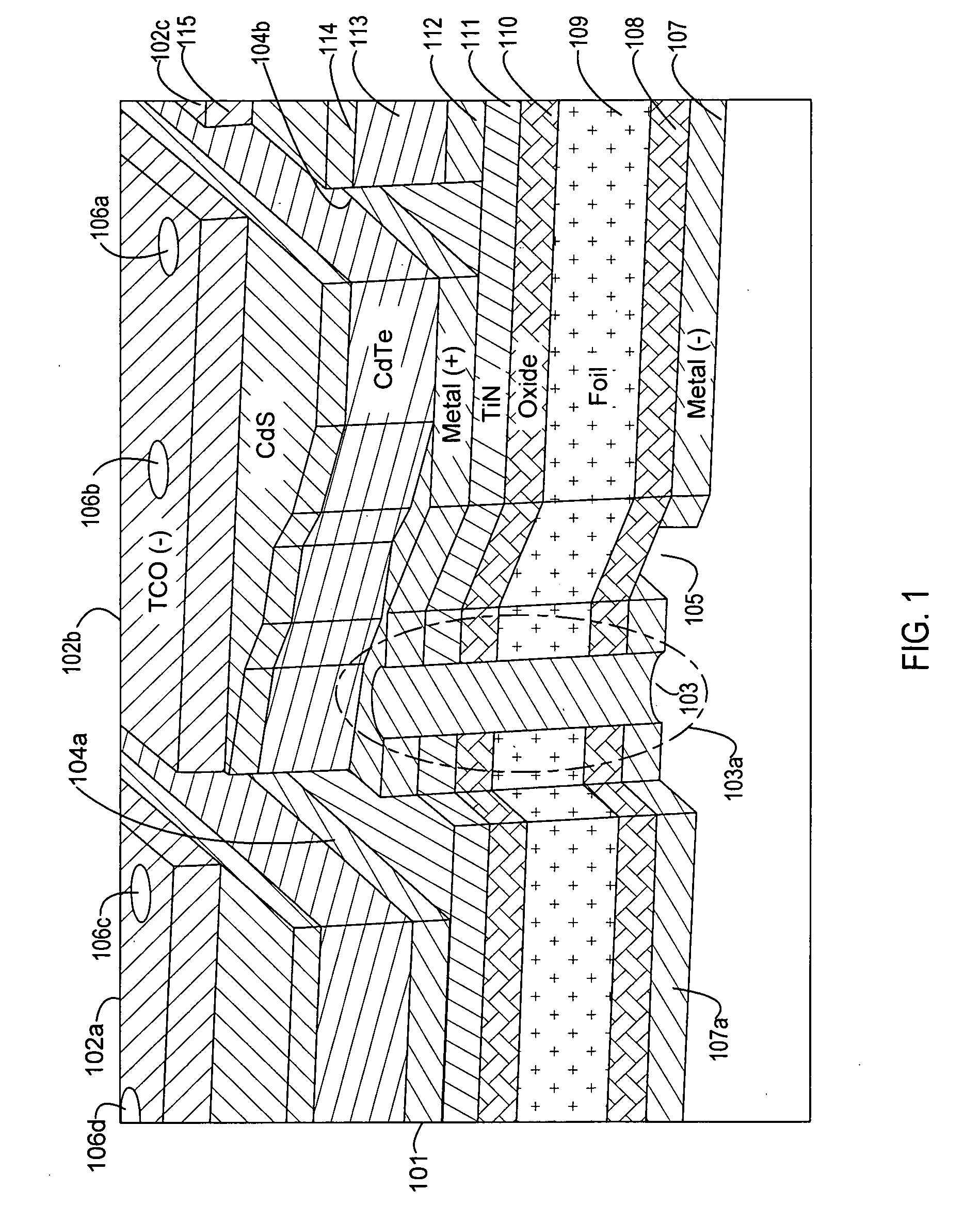
[0065]With reference to FIG. 1 there is shown a cross section of a photovoltaic device 101 in accordance with one embodiment of the present invention. Photovoltaic cells 102a, 102b and 102c are shown and adjacent cells 102a and 102b are interconnected with a serial interconnect via 103. Detail of via 103a is expanded in FIG. 2B. Scribes 104a and 104b separate photovoltaic cells 102a and 102b. Scribe 104a through the bottom electrode 112 in conjunction with scribe 105 in the back contact 107 serve to electrically isolate adjacent cells, connected by interconnect via 103. Scribe 104a is near via 103 and isolates via 103 from electrical contact with cell 102a bottom electrode, but makes electrical contact with cell 102a via an electrical contact with the bottom electrode of cell 102b through via 103 contact(not shown) to the back electrode 107a of cell 102a. Holes 106a and 1...
example 2
A Thin-Film CdTe Solar Cell on a Flexible Insulating Substrate with Serial Interconnects and a Back Metal Contact with Filled Vias
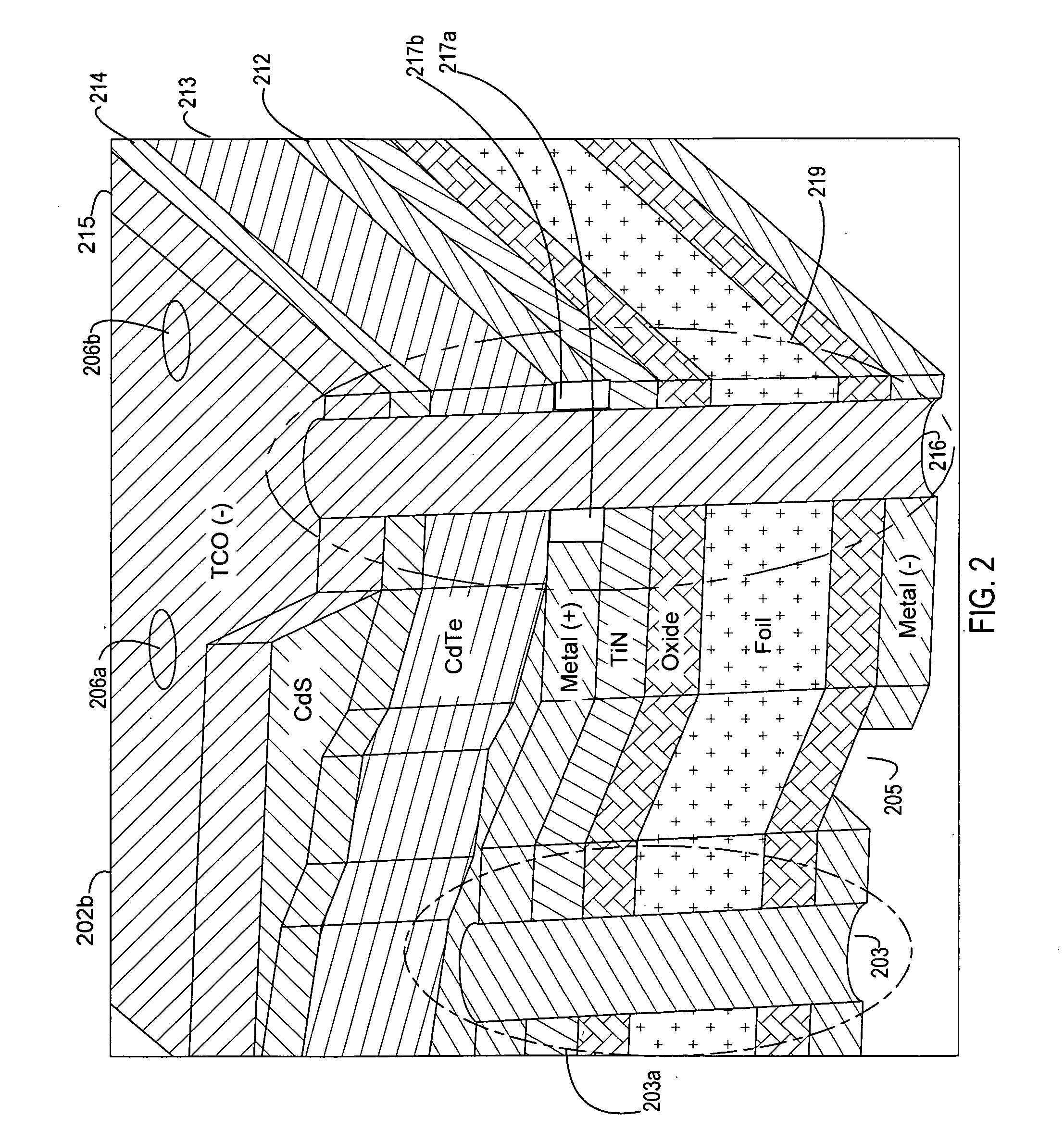
[0066]A process for manufacturing a solar cell in accordance with the present invention is described with particular reference to FIGS. 1-3. An insulating substrate 109 is provided with a plurality of holes 106a, 106b, 106c and 106d having a set of diameters. The holes may be created by any manner suitable depending on the material and size, shape and number of holes. The distance between the holes is variable. In one embodiment serial interconnect holes are punched 10 cm apart transversely on a foil in rows separated 100 cm apart in the orthogonal or longitudinal direction. Rows of current collection holes are punched in between the rows of serial connection holes at a separation of 1 cm in both the x and y directions. It is preferable to minimize the distance between the current collect vias to minimize resistance but to also minimize the number of cont...
example 3
A Thin-Film CdTe Solar Cell on a Flexible Conducting Substrate with Serial Interconnects and a Back Metal Contact
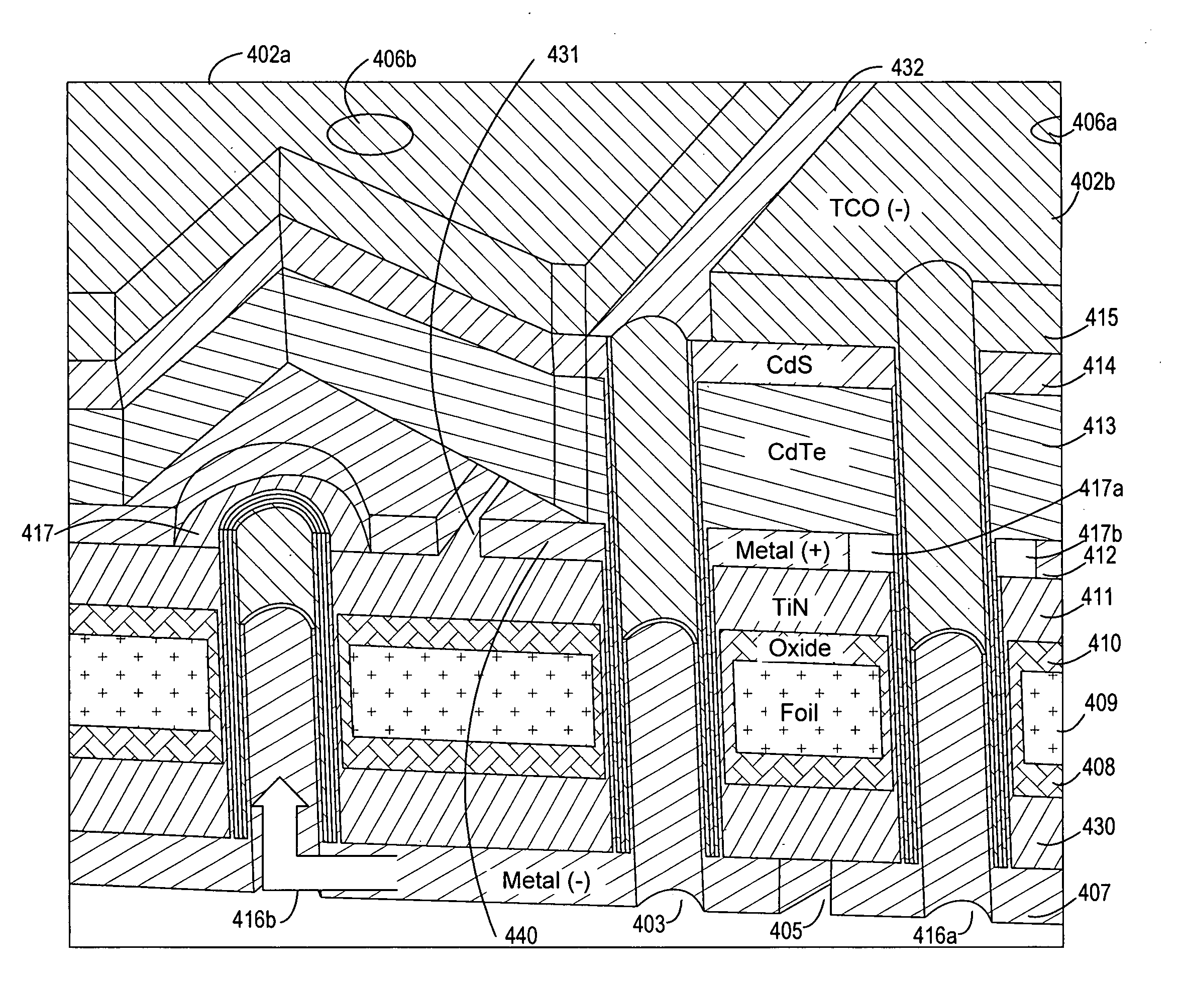
[0075]With reference to FIG. 4 there is disclosed a photovoltaic device designed in accordance with one embodiment of the present invention having photovoltaic cell 402a and adjacent photovoltaic cell 402b connected by serial interconnect via 403. Each cell 402a and 402b preferably has at least the following layer structure in order from bottom to top: a back metal electrode 407, a lower barrier layer 430, a lower oxide layer 408, a substrate 409, a top oxide layer 410, a top barrier layer 411, a bottom electrode 412, an absorber layer 413, a window layer 414 and a transparent conductor layer 415. Holes 406a and 406b define the openings at the top of current collection vias 416a and 416b respectively. Current collection vias 416a and 416b are in adjacent photovoltaic cells 402b and 402a respectively and serially interconnected by serial connection via 403. Back electrode ...
PUM
 Abstract
Description
Claims
Application Information
 - R&D
- Intellectual Property
- Life Sciences
- Materials
- Tech Scout
- Unparalleled Data Quality
- Higher Quality Content
- 60% Fewer Hallucinations
Browse by: Latest US Patents, China's latest patents, Technical Efficacy Thesaurus, Application Domain, Technology Topic, Popular Technical Reports.
© 2025 PatSnap. All rights reserved.Legal|Privacy policy|Modern Slavery Act Transparency Statement|Sitemap|About US| Contact US: help@patsnap.com