Method for manufacturing a solid-state image capturing apparatus, and electronic information device

a solid-state image and capturing apparatus technology, applied in the direction of photomechanical apparatus, instruments, photosensitive materials, etc., can solve the problems of increasing the number of white defects in the manufactured white defects or dark current may get worse, and achieve the effect of reducing damage, effectively preventing white defects and dark current, and improving the yield rate of the solid-state image capturing apparatus

Inactive Publication Date: 2009-10-15
SHARP KK
View PDF13 Cites 13 Cited by
  • Summary
  • Abstract
  • Description
  • Claims
  • Application Information

AI Technical Summary

Benefits of technology

[0031]The present invention is intended to solve the conventional problems described above. The objective of the present invention is to provide a method for manufacturing a solid-state image capturing apparatus, in which iodine, which is a constituent element of a photo-acid-generating agent of an impurity implantation preventing film, is prevented from being implanted from the impurity implantation preventing film, such as a chemical amplification type resist film, which is used as an implantation mask of impurity, into a photodiode section formed in a substrate, thereby reducing the occurrence of white defects and dark current due to crystal defect in the photodiode section and improving the yield rate of the solid-state image capturing apparatus. Further, the objective of the present invention is to provide an electronic information device having therein the solid-state image capturing apparatus obtained by the method for manufacturing a solid-state image capturing apparatus.
[0057]According to the present invention, what is used as a resist material for a resist mask (impurity implantation preventing film) for preventing the implantation of an impurity, is a resist material that is obtained by replacing at least a portion of iodonium salt contained in a chemical amplification type resist with a photo-acid-generating agent which does not contain iodine, the chemical amplification type resist containing iodonium salt, which is a photo-acid-generating agent, of the content determined based on at least the wavelength of an exposure light and the film thickness of the resist mask, thereby reducing the damage due to the penetration of iodine from a photoresist film used as an impurity implantation preventing film into a photodiode section (photoelectric conversion section) so as to effectively prevent white defects and dark current from occurring and to improve the yield rate of the solid-state image capturing apparatus.
[0058]Further, according to the present invention, when at least one impurity implantation area of an electric charge transfer section, an electric charge readout section for reading out a signal charge from a photoelectric conversion section to the electric charge transfer section, and a channel stop section for electrically separating the photoelectric conversion section from the electric charge transfer section, which are in the vicinity of the photodiode section (photoelectric conversion section), is formed, a resist mask composed of a chemical amplification type resist in which the content of a photo-acid-generating agent including iodine is limited, is used as described above. Therefore, when the impurity implantation area is formed, it is possible to reduce the damage due to the penetration of iodine from the resist mask used as an impurity implantation preventing film into the photodiode section (photoelectric conversion section).
[0059]Further, according to the present invention, since an insulating hard mask is used as an impurity implantation preventing film for preventing the impurity implantation, the damage due to the penetration of iodine from the resist mask used as an impurity implantation preventing film into the photodiode section (photoelectric conversion section) is prevented, thereby effectively preventing white defects and dark current from occurring and improving the yield rate of the solid-state image capturing apparatus.
[0060]According to the present invention as described above, in a method for manufacturing the solid-state image capturing apparatus when an impurity implantation area that constitutes a photodiode section in a pixel is formed, a resist material obtained by replacing at least a portion of iodonium salt contained in a chemical amplification type resist containing iodonium salt, which functions as a photo-acid-generating agent, of the content determined based on at least the wavelength of an exposure light and the film thickness of the resist mask with a photo-acid-generating agent without iodine is used as a resist material for a resist mask (impurity implantation preventing film) for preventing the implantation of an impurity. Therefore, the damage to the atom configuration due to the penetration of iodine is reduced in the vicinity of the boarder of the photodiode section (photoelectric conversion section) in the substrate, and as a result, it is possible to effectively prevent white defects and dark current from occurring to improve the yield rate of the solid-state image capturing apparatus.
[0061]Further, according to the present invention, in a method for manufacturing the solid-state image capturing apparatus when an impurity implantation area that constitutes a photodiode section in a pixel is formed, an insulating hard mask, which is patterned by a photolithography technique as an impurity implantation preventing layer for preventing the impurity implantation, is used. Therefore, the damage to the atom configuration due to the penetration of iodine is avoided in the vicinity of the boarder of the photodiode section (photoelectric conversion section) in the substrate, and as a result, it is possible to effectively prevent white defects and dark current from occurring to improve the yield rate of the solid-state image capturing apparatus.

Problems solved by technology

In a case where an impurity implantation area that constitutes a photodiode section (photoelectric conversion section) and an impurity implantation area adjacent to the photodiode section (e.g., channel stop section) are formed as described above, when a photoresist film is used as an impurity implantation mask for the purpose of preventing the impurity from being implanted, on a portion where an impurity implantation area is not formed in a substrate, white defects or dark current may get worse if the photoresist film is mixed with iodonium salt, as onium salt which is a photo-acid-generating agent.
As described above, as the content ratio of the iodonium salt increases in the chemical amplification type resist used for the manufacturing of a solid-state image capturing apparatus, an increase in the number of white defects in the manufactured solid-state image capturing apparatus occurs.

Method used


Image

  • Method for manufacturing a solid-state image capturing apparatus, and electronic information device
  • Method for manufacturing a solid-state image capturing apparatus, and electronic information device
  • Method for manufacturing a solid-state image capturing apparatus, and electronic information device

Examples


embodiment 1

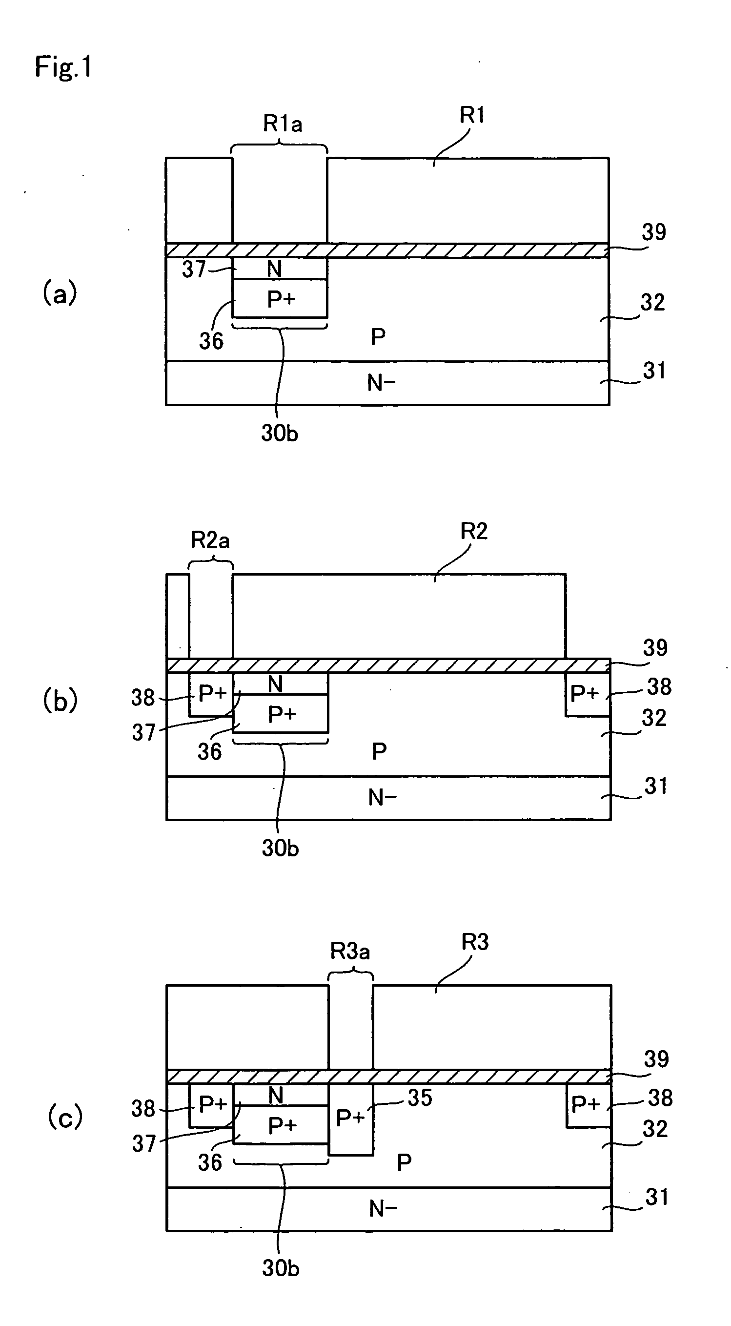
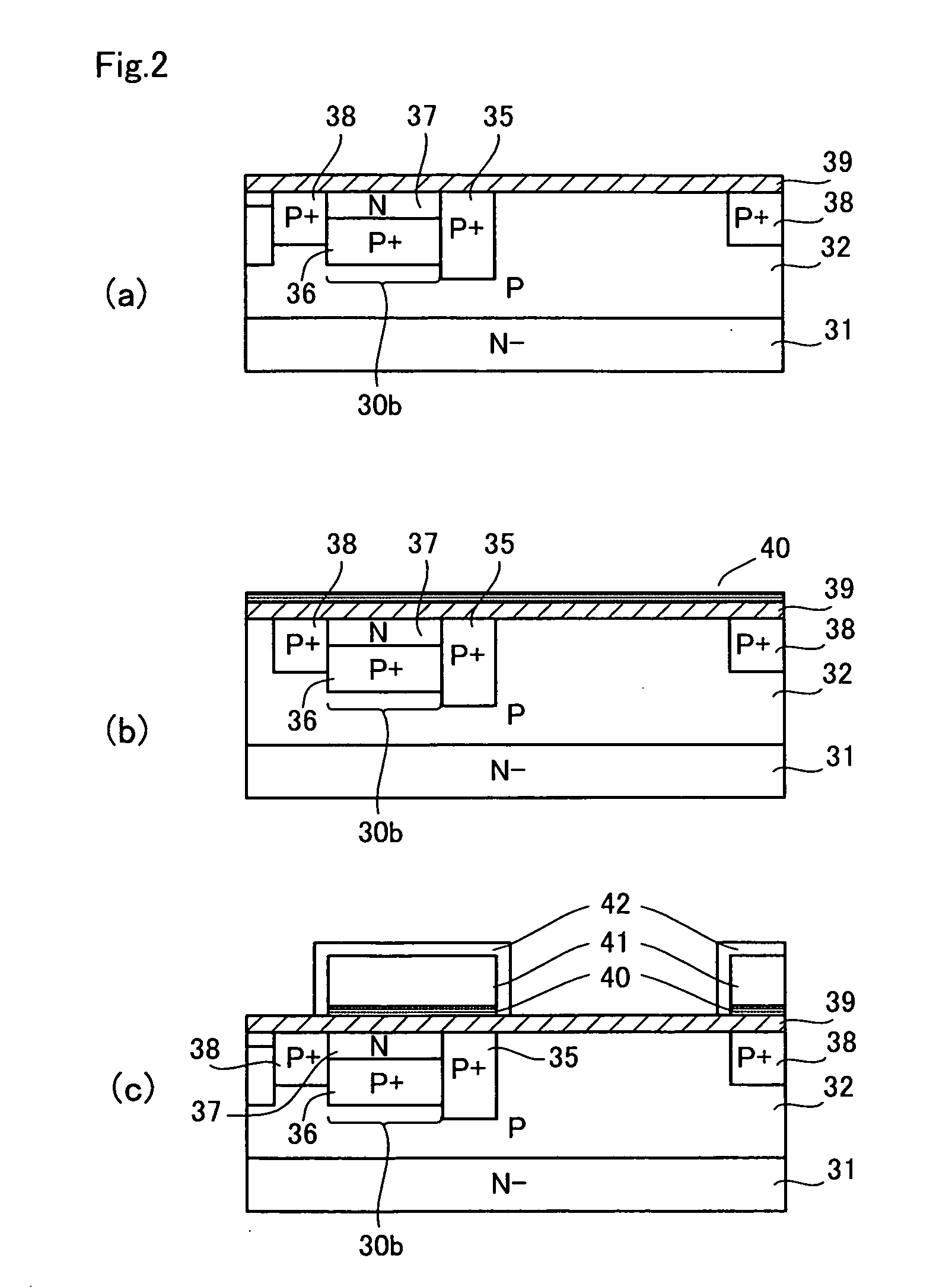
[0101]FIGS. 1 through 3 are diagrams illustrating a method for manufacturing a solid-state image capturing apparatus according to Embodiment 1 of the present invention. FIGS. 1(a) to 1(c) illustrate a process for forming an impurity diffusion area where a vertical CCD section is configured, in a surface area of a semiconductor substrate, in the order of the steps. FIGS. 2(a) to 2(c) illustrate a process for forming a transfer electrode where a vertical CCD section is configured, in a surface area of a semiconductor substrate, in the order of the steps.

[0102]FIGS. 3(a) and 3(b) illustrate a process for forming an impurity diffusion area where a photodiode is configured in a surface area of a semiconductor substrate. FIG. 3(c) illustrates a forming process of a planarization film.

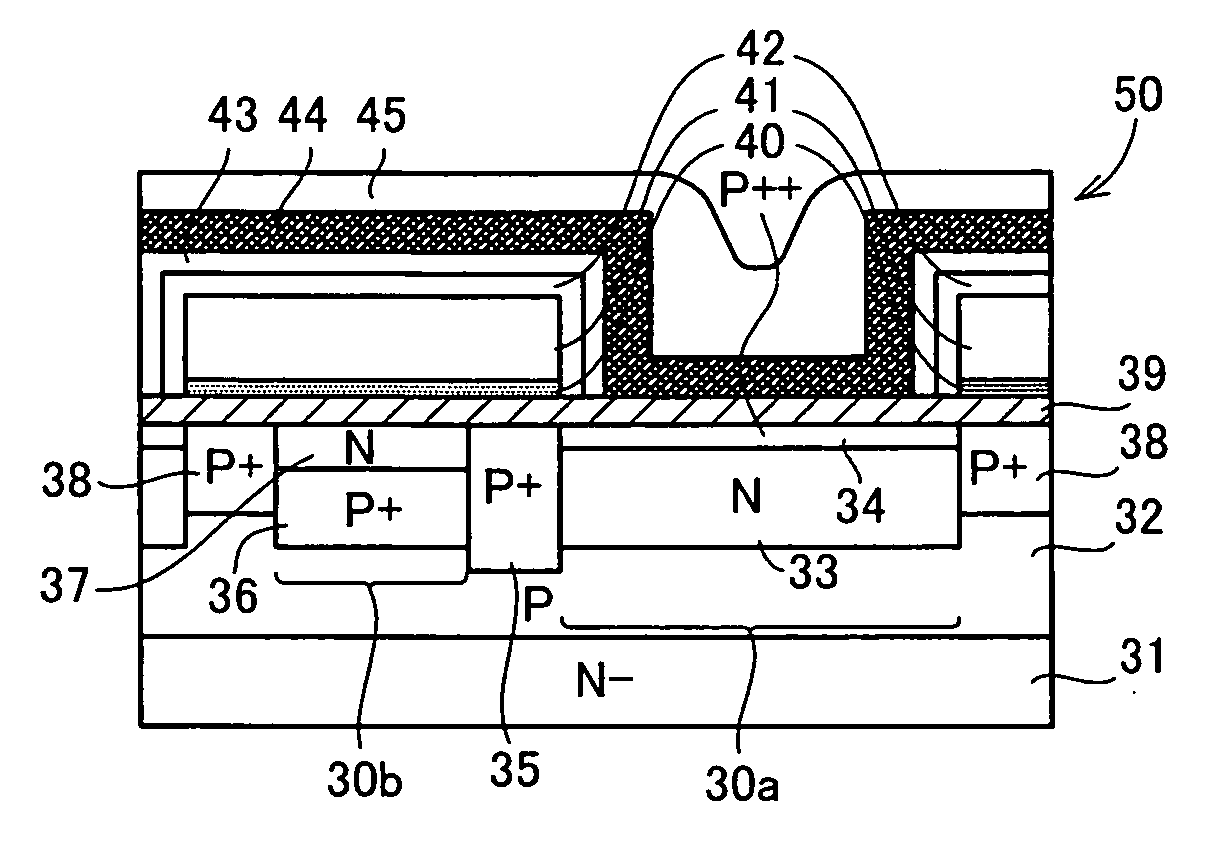
[0103]As illustrated in FIG. 3(c), a solid-state image capturing apparatus 50 manufactured by the method for manufacturing a solid-state image capturing apparatus according to Embodiment 1 includes: a plurali...

embodiment 2

[0162]Although not specifically described in the embodiment described above, an electronic information device having an image input device will be described hereinafter as Embodiment 2 of the present invention. The electronic information device having an image input device, such as a digital camera (e.g., digital video camera and digital still camera), an image input camera, a scanner, a facsimile machine and a camera-equipped cell phone device, includes an image capturing section using the solid-state image capturing apparatus according to the embodiment described above.

[0163]FIG. 15 is a block diagram illustrating an exemplary diagrammatic structure of an electronic information device, as Embodiment 2 of the present invention, using the solid-state image capturing apparatus according to Embodiment 1 of the present invention as an image input device in an image capturing section.

[0164]The electronic information device 90 according to Embodiment 2 of the present invention as illustr...


PUM


Abstract

A method for manufacturing a solid-state image capturing apparatus including a pixel array constituted of a plurality of pixels, is provided, where each of the plurality of pixels includes a photoelectric conversion section, the method comprising the steps of: forming an impurity diffusion area in a surface area of a semiconductor substrate; and forming a plurality of different impurity diffusion areas in the surface area of the semiconductor substrate, other than the impurity diffusion area constituting the photoelectric conversion section.

Description

[0001]This nonprovisional application claims priority under 35 U.S.C. §119(a) to Patent Application No. 2008-105106 filed in Japan on Apr. 14, 2008, the entire contents of which are hereby incorporated by reference.BACKGROUND OF THE INVENTION[0002]1. Field of the Invention[0003]The present invention relates to a method for manufacturing a solid-state image capturing apparatus, and to an electronic information device; and particularly to a method for forming a photoresist mask in a method for manufacturing various solid-state image capturing apparatuses, such as a CCD type image sensor and a CMOS type image sensor, and an electronic information device having therein the solid-state image capturing apparatus obtained by the method for manufacturing a solid-state image capturing apparatus.[0004]2. Description of the Related Art[0005]A conventional solid-state image capturing apparatus, such as a CCD image sensor, generally includes a pixel array constituted of a plurality of pixels, th...

Claims


Application Information

Patent Timeline
Patent Type & Authority Applications(United States)
IPC IPC(8): H01L21/265H01L31/18
CPCG03F7/0045G03F7/0392H01L29/66946H01L27/14806H01L27/14689
Inventor HATAI, TETSUYA
Owner SHARP KK
Why Eureka
Try Eureka