Unipolar semiconductor photodetector with suppressed dark current and method for producing the same
a photodetector and semiconductor technology, applied in the field of photodiodes, can solve the problems of cumbersome and expensive means for cooling and maintaining such a low temperature in photodiodes, reducing noise to a limited value, and limiting the signal-to-noise ratio which can be obtained from photodiodes (and many other electronic components)
- Summary
- Abstract
- Description
- Claims
- Application Information
AI Technical Summary
Benefits of technology
Problems solved by technology
Method used
Image
Examples
embodiment 1
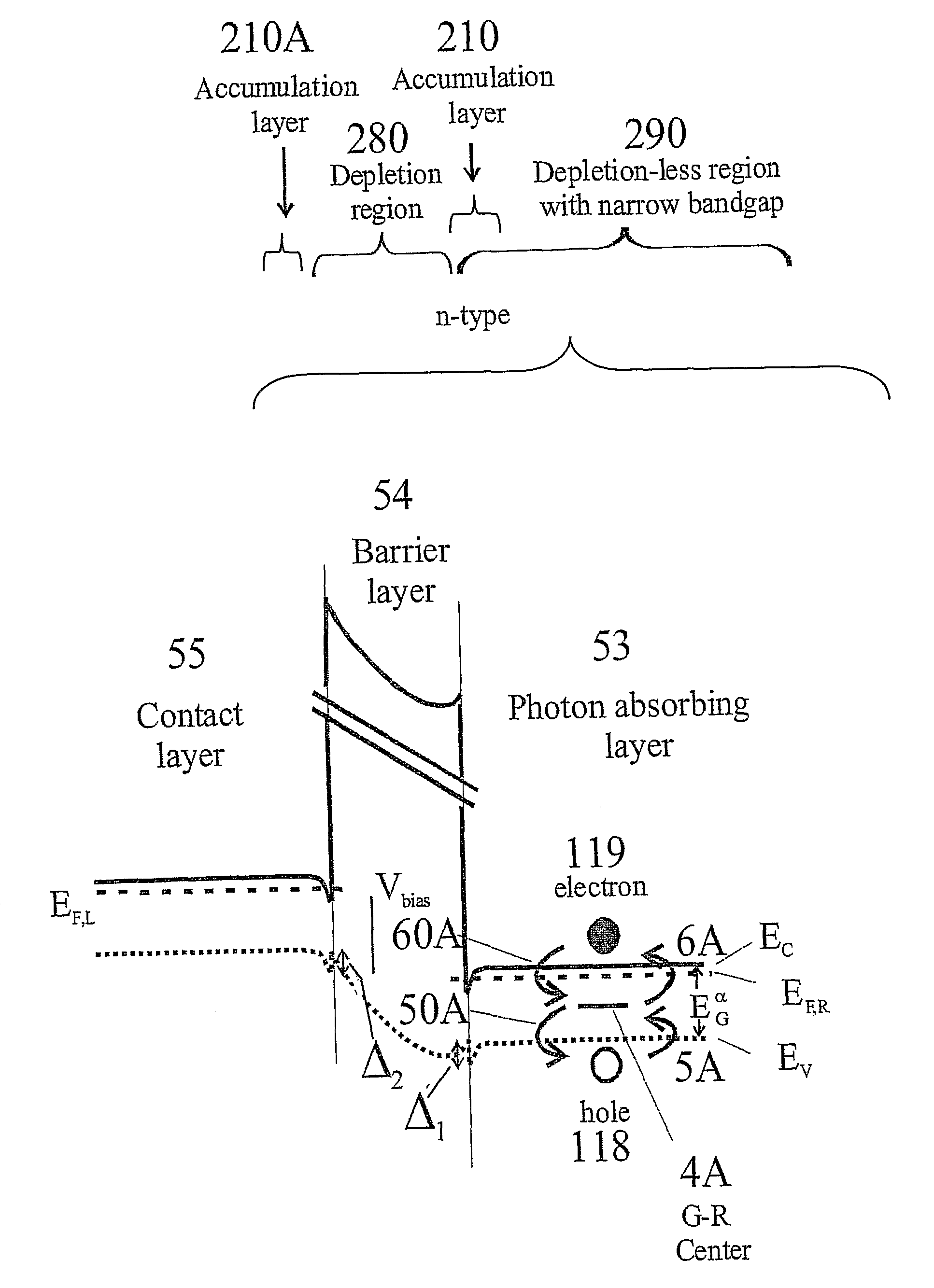
[0099]A band diagram of a first embodiment of the invention is shown in FIG. 4a. Examples of the structure of said first embodiment are shown in FIGS. 4b and 4c. In the first embodiment, band bending is allowed in the barrier layer 24 and a short distance into the contact layer 75. Band bending in the contact layer 75 is usually due to electron accumulation close to the barrier (210A in FIG. 3a). The bands in the photon absorbing layer 23 are flat at the maximum operating bias but a small accumulation layer of electrons (210 in FIG. 3a) forms close to the barrier layer at lower bias, as shown in FIG. 4a.
[0100]The n-type photon-absorbing layer 23 is made of InAsSb alloy. The doping is typically in the range of n16 cm−3 and the thickness is typically in the range 1-10 μm.
[0101]The use of InAsSb enables operation in the MWIR atmospheric transmission window (3-5 μm).
[0102]The contact layer 75 is made of n-type InAsSb with typical values of doping in the range 5×101416 cm−3 and thicknes...
embodiment 2
[0106]A band diagram of a second embodiment of the invention is shown in FIG. 5a. An example of the structure of said second embodiment is shown in FIG. 5b. The n-type photon-absorbing layer 23 is made of InAsSb alloy. The doping is typically in the range n16 cm−3, and the thickness of the photon-absorbing layer 23 is typically in the range 1-10 μm. The use of InAsSb enables operation in the MWIR atmospheric transmission window (3-5 μm). The contact layer 75 is made of n-type InAsSb with typical values of doping in the range 5×101416 cm−3 and thickness>0.1 μm.
[0107]The barrier layer 74 is made of GaAlSbAs alloy with thickness values typically in the range 0.05-1 μm. The barrier layer 74 is a p-type material, with a typical doping range of 1×10¹⁴≦p17 cm−3. A depletion region exists in the GaAlSb barrier layer 74 but not in the photon absorbing layer 23. The depletion region exists in the barrier layer but its electric field is allowed to extend a short distance into the n-type contac...
embodiment 3
[0109]A band diagram of a third embodiment of the invention is shown in FIG. 6a. An example of the structure of said third embodiment is shown in FIG. 6b.
[0110]The n-type photon-absorbing layer 83 and the n-type contact layer 85 are both made from type II superlattice materials that comprise alternating sub-layers of InAs and Ga1-xInxSb (or alternating sub-layers of closely related semiconductor alloys, e.g. InAs1-wSbwGa1-x-yInxAlySb1-zAsz, etc. with 0≦w≦1, 0≦x≦1, 0≦y≦1, 0≦z≦1 and x+y83 the average doping over many sub-layers of the superlattice is typically in the range n16 cm−3, and the thickness of the whole superlattice region is typically in the range 1-10 μm.
[0111]As known in the art, the use of a type II InAs / InGaSb (or closely related) superlattice material enables operation in both the Mid-Wave Infra-Red (MWIR: 3-5 μm) and in the Long-Wave Infra-Red (LWIR: 8-12 μm) terrestrial atmospheric transmission windows, and also in the Very Long-Wave Infra-Red (VLWIR: 12-20 μm) rang...
PUM
 Abstract
Description
Claims
Application Information
 - R&D
- Intellectual Property
- Life Sciences
- Materials
- Tech Scout
- Unparalleled Data Quality
- Higher Quality Content
- 60% Fewer Hallucinations
Browse by: Latest US Patents, China's latest patents, Technical Efficacy Thesaurus, Application Domain, Technology Topic, Popular Technical Reports.
© 2025 PatSnap. All rights reserved.Legal|Privacy policy|Modern Slavery Act Transparency Statement|Sitemap|About US| Contact US: help@patsnap.com


