Multilayer wiring board and method of manufacturing the same

a wiring board and multi-layer technology, applied in the direction of printed circuit aspects, printed circuit non-printed electrical components association, conductive pattern formation, etc., can solve the problem of disturbance of the increase in speed, the pitch of the terminals on the ic chip and the mother board side is large, and it is difficult to directly connect the ic chip onto the mother board. , to achieve the effect of increasing the adhesion strength of the via conductor and enhancing the product yield

Active Publication Date: 2009-09-24
NGK SPARK PLUG CO LTD
View PDF14 Cites 11 Cited by
  • Summary
  • Abstract
  • Description
  • Claims
  • Application Information

AI Technical Summary

Benefits of technology

The present invention provides a multilayer wiring board with increased adhesion strength and enhanced electrical characteristics. The board has a reduced thickness and wiring length, and includes a laminated structure with alternating conductor layers and insulating layers. The insulating layer contains a fiber material in a polymeric material, which increases the strength of the board. The fiber protrudes from the internal wall surface of the via hole, preventing adhesion failure and cracking. The conductor layers are pattern-formed on the insulating layer using a metallic material. The insulating layer can be selected based on its insulating property, heat resistance, or moisture resistance. The method of manufacturing the board includes steps of forming an insulating layer with a sheet-shaped buildup material containing a fiber material in a polymeric material, irradiating a laser beam to form via holes, selectively removing the polymeric material in the internal wall surface of the via hole to protrude the fiber tip, and carrying out plating to form filled via conductors.

Problems solved by technology

However, a great difference is made in a pitch between the terminals on the IC chip and the mother board side.
Therefore, it is hard to directly connect the IC chip onto the mother board.
In this case, the wiring penetrating the core board contributes as a high inductance so that a transmission loss of a radio frequency signal or a circuit malfunction is caused, resulting in a disturbance of the increase in the speed.
Since the coreless wiring board is manufactured through the omission of the core board, however, a strength thereof cannot be maintained sufficiently.
There is a high possibility that an adhesion failure or a via slip-off of a via conductor for connecting the conductor layers in the buildup layer might be caused in the case in which an excessive stress is applied to the wiring board due to the warpage.
As a result, a product yield of the coreless wiring board is deteriorated.

Method used


Image

  • Multilayer wiring board and method of manufacturing the same
  • Multilayer wiring board and method of manufacturing the same
  • Multilayer wiring board and method of manufacturing the same

Examples


Embodiment Construction

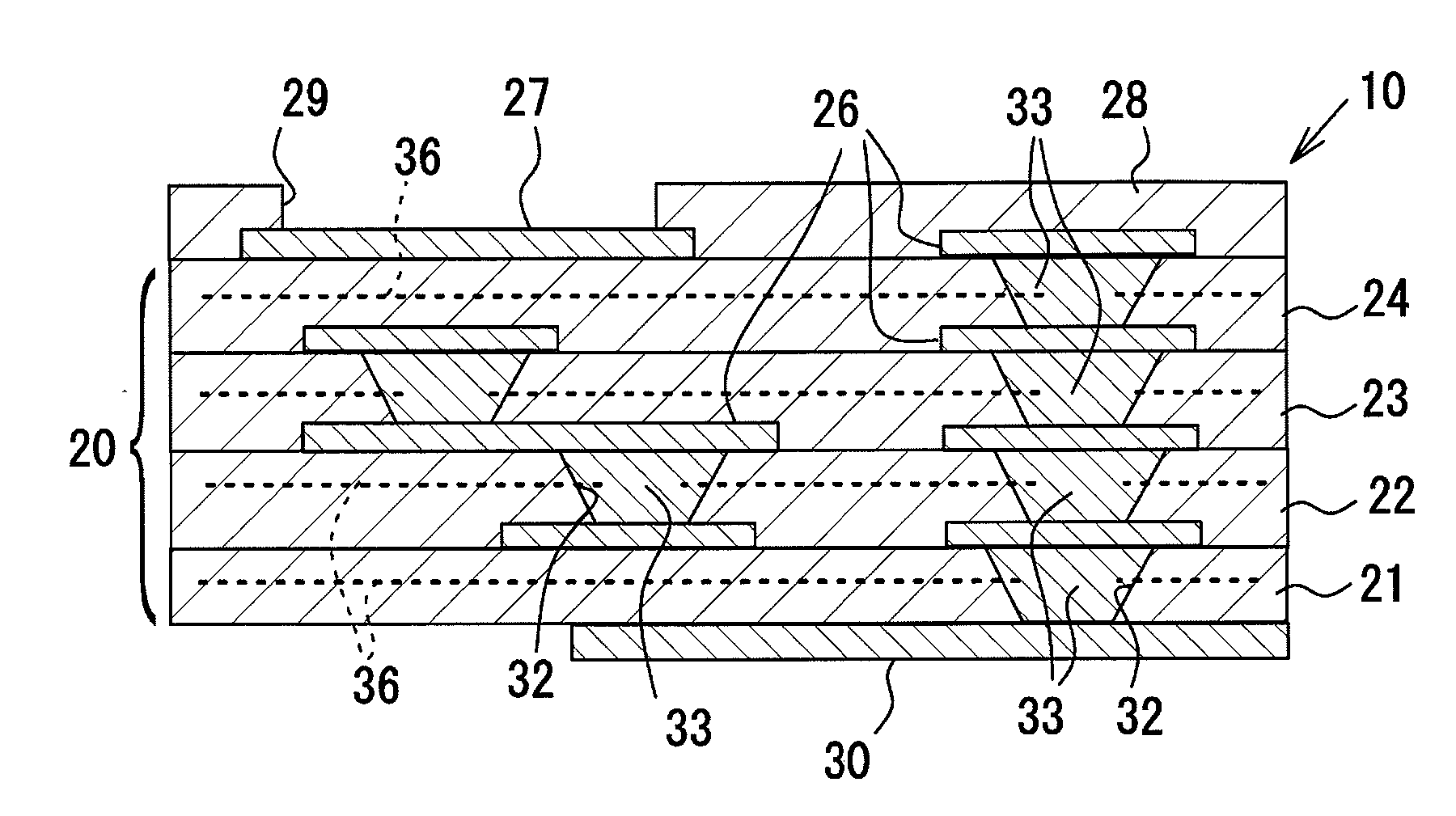
[0038]An embodiment according to the invention will be described below in detail with reference to the drawings. FIG. 1 is an enlarged sectional view showing a schematic structure of a coreless wiring board (a multilayer wiring board) according to the embodiment and FIG. 2 is a plan view showing the coreless wiring board.

[0039]As shown in FIG. 1, a coreless wiring board 10 has no core board but a wiring laminated portion 20 (a laminated structure) in which four resin insulating layers (insulating layers) 21, 22, 23 and 24 formed of an epoxy resin and a conductor layer 26 formed of copper are alternately laminated into a multilayer. In the coreless wiring board 10, a terminal pad 27 is provided on a surface (an upper surface) of the resin insulating layer 24 to be the fourth layer. FIG. 1 is a sectional view showing a part of the coreless wiring board 10. A plurality of terminal pads 27 is disposed in an array on an upper surface of the coreless wiring board 10, for example (see FIG....


PUM

PropertyMeasurementUnit
diameteraaaaaaaaaa
diameteraaaaaaaaaa
thicknessaaaaaaaaaa

Abstract

A coreless wiring board has no core board but a laminated structure in which a conductor layer and resin insulating layers are alternately laminated into a multilayer. Each of the resin insulating layers is formed to contain a glass cloth in an epoxy resin. A plurality of via holes is formed to penetrate each of the resin insulating layers, and a filled via conductor for electrically connecting the conductor layers is formed in the via holes respectively. A tip of the glass cloth contained in each of the resin insulating layers is protruded from an internal wall surface of the via hole and cuts into a sidewall of the filled via conductor.

Description

CROSS-REFERENCE TO RELATED APPLICATIONS[0001]This application is based upon and claims priority from Japanese Patent Application No. 2008-064985 filed on Mar. 13, 2008, the entire contents of which are incorporated herein by reference.BACKGROUND OF THE INVENTION[0002]1. Field of the Invention[0003]The present disclosure relates to a multilayer wiring board having no core board but a laminated structure in which a conductor layer and an insulating layer are alternately laminated into a multilayer, and a method of manufacturing the multilayer wiring board.[0004]2. Description of Related Art[0005]In recent years, a semiconductor integrated circuit device (an IC chip) to be used as a microprocessor of a computer has increasingly been enhanced in a speed and a function, and incidentally, there is a tendency that the number of terminals is increased and a pitch between the terminals is also reduced. In general, a large number of terminals are densely disposed in an array on a bottom face ...

Claims


Application Information

Patent Timeline
Patent Type & Authority Applications(United States)
IPC IPC(8): H05K1/11H05K3/00
CPCH05K1/0366H05K3/0035H05K3/0055H05K3/025Y10T29/49155H05K3/4682H05K2201/09563H05K2203/0152Y10T29/49165H05K3/421
Inventor KATAGIRI, HIROSHIASANO, TOSHIYA
Owner NGK SPARK PLUG CO LTD
Why Eureka
Try Eureka