Thin film transistor, manufacturing method thereof, display device, and manufacturing method thereof

Inactive Publication Date: 2009-09-10
SEMICON ENERGY LAB CO LTD
View PDF15 Cites 25 Cited by
  • Summary
  • Abstract
  • Description
  • Claims
  • Application Information

AI Technical Summary

Benefits of technology

[0011]In view of the above problems, an object of an embodiment of the invention is to provide a new method for manufacturing a thin film transistor which requires no additional photomask for patterning a gate electrode layer. Namely, a manufacturing method is disclosed, which enables the manufacture of a thin film transistor without a complicated technique even if only a single photomask is employed.
[0047]Furthermore, since a thin film transistor in which leakage current generated at an end portion of the gate electrode layer is low can be manufactured, a display device with a high contrast ratio and favorable display quality can be obtained.

Problems solved by technology

However, even in the case where a bottom gate thin film transistor is manufactured using the above multi-tone mask, at least two photomasks are required, and it is difficult to further reduce the number of photomasks.

Method used


Image

  • Thin film transistor, manufacturing method thereof, display device, and manufacturing method thereof
  • Thin film transistor, manufacturing method thereof, display device, and manufacturing method thereof
  • Thin film transistor, manufacturing method thereof, display device, and manufacturing method thereof

Examples


embodiment 1

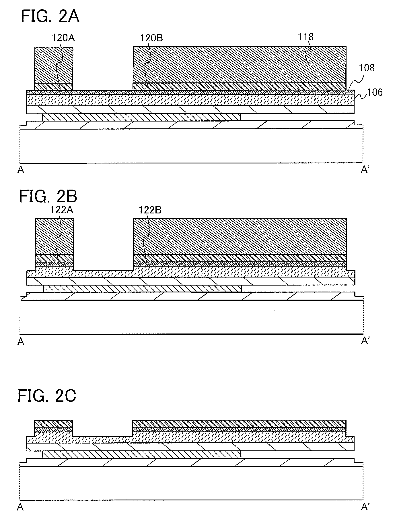
[0093]In Embodiment 1, an example of a manufacturing method of a thin film transistor and a manufacturing method of a display device in which the thin film transistors are arranged in matrix will be described with reference to FIG. 1A to FIG. 25B-2.

[0094]FIG. 16 to FIG. 20 are top views of thin film transistors according to this embodiment. FIG. 20 is a completion drawing in the situation that formation of a pixel electrode is finished. FIG. 1A to FIG. 3C are cross-sectional views taken along the line A-A′ in FIG. 16 to FIG. 20. FIG. 4A to FIG. 6C are cross-sectional views taken along the line B-B′ in FIG. 16 to FIG. 20. FIG. 7A to 9C are cross-sectional views taken along the line C-C′ in FIG. 16 to FIG. 20. FIG. 10A to FIG. 12C are cross-sectional views taken along the line D-D′ in FIG. 16 to FIG. 20. FIG. 13A to FIG. 15C are cross-sectional views taken along the line E-E′ in FIG. 16 to FIG. 20.

[0095]First, a first insulating film 101, a first conductive film 102, a second insulati...

embodiment 2

[0203]In Embodiment 2, a manufacturing method of a thin film transistor and a manufacturing method of a display device according to one embodiment of the invention disclosed in this specification, which are different from those of Embodiment 1, will be described. Specifically, a manufacturing method of a thin film transistor which is similar to that of Embodiment 1, without using a multi-tone mask will be described with reference to FIGS. 26A to 26C, FIGS. 27A to 27C, FIG. 28, FIG. 29, and FIG. 30.

[0204]FIGS. 26A, 26B, and 26C correspond to FIG. 1A, FIG. 1C, and FIG. 2A of Embodiment 1. FIGS. 27A, 27B, and 27C correspond to FIG. 10A, FIG. 10C, and FIG. 11A of Embodiment 1. FIG. 28, FIG. 29, and FIG. 30 correspond to FIG. 16, FIG. 17, and FIG. 18 of Embodiment 1. The cross-sectional views taken along the line A-A′ illustrated in FIG. 28, FIG. 29, and FIG. 30 correspond to FIGS. 26A, 26B, and 26C, and the cross-sectional views taken along the line D-D′ illustrated in FIG. 28, FIG. 29,...

embodiment 3

[0218]In Embodiment 3, an example of a manufacturing method of a thin film transistor and a manufacturing method of an EL display device in which the thin film transistors are arranged in matrix will be described with reference to FIG. 31 to FIG. 39C and FIG. 43A to FIG. 43C.

[0219]Various pixel circuits for EL display devices (active EL display devices) which use thin film transistors as switching elements are considered. FIG. 31 illustrates an example of a simple pixel circuit, and a manufacturing method of a pixel structure using this pixel circuit will be described in this embodiment. However, the pixel circuit of the EL display device disclosed in this specification is not limited to the one having the configuration illustrated in FIG. 31.

[0220]In the pixel structure of the EL display device illustrated in FIG. 31, a pixel 191 includes a first transistor 181, a second transistor 182, a third transistor 183, a capacitor 184, and a light-emitting element 185. The first, second, an...


PUM


Abstract

Disclosed is a manufacturing method of a thin film transistor, which enables the formation of a thin film transistor by using only one photomask. The method includes: over a substrate sequentially forming a first insulating film, a first conductive film, a second insulating film, a semiconductor film, an impurity semiconductor film, and a second conductive film; forming a resist mask thereover using a first photomask; performing a first etching to allow the side surface of the layers including an upper portion of the first insulating film, the first conductive film, the second insulating film, the semiconductor film, the impurity semiconductor film, and the second conductive film to be coplanar to a side surface of the resist mask; and performing a second etching to selectively etch the first conductive film to allow the side surface of the first conductive film is located inside the side surface of the layers.

Description

BACKGROUND OF THE INVENTION[0001]1. Field of the Invention[0002]The present invention relates to a thin film transistor, a manufacturing method thereof, a display device including the thin film transistor, and a manufacturing method thereof.[0003]2. Description of the Related Art[0004]In recent years, thin film transistors that are formed using a semiconductor thin film having a thickness of several nanometers to several hundreds of nanometers over a substrate having an insulating surface such as a glass substrate have been attracting attentions. Thin film transistors are widely used for electronic devices such as ICs (integrated circuits) and electro-optical devices. In particular, rapid development of thin film transistors as switching elements of image display devices typified by liquid crystal display devices, EL (electro luminescence) display devices, and the like has been demanded. In an active matrix liquid crystal display device, a voltage is applied to a pixel electrode con...

Claims


Application Information

Patent Timeline
IPC IPC(8): H01L21/70
CPCH01L21/764H01L27/1288H01L27/1214H01L29/42384H01L29/6675
Inventor MIYAIRI, HIDEKAZU
Owner SEMICON ENERGY LAB CO LTD
Why Eureka
Try Eureka