Vcsel with reduced light scattering within optical cavity

Inactive Publication Date: 2009-08-27
SUMITOMO ELECTRIC IND LTD
View PDF2 Cites 9 Cited by
  • Summary
  • Abstract
  • Description
  • Claims
  • Application Information

AI Technical Summary

Benefits of technology

[0007]The VCSEL of the present invention has a feature that the only the heavily doped p-type layer forms a mesa, and the heavily doped n-type layer covers this mesa. Although a step is appeared on the surface of the first n-type spacer layer provided on the heavily doped n-type layer as reflecting the heavily doped p-type mesa, a height of this step is comparatively small because the step only reflects the mono-layer of the heavily doped p-type mesa. Therefore, the light scattering by this step formed between the n-type spacer layer and the second DBR may be suppressed in spite of the unevenness within the optical cavity.
[0008]In the VCSEL of the invention, the heavily doped p-type mesa only covers the first area of the p-type spacer layer and the heavily doped n-type layer covers the second area. The light absorption due to the n-type layer is generally insensitive to the doping density thereof compared to the p-type layer, because the free electron absorption becomes dominant in the n-type layer, while, the inter-band transition is dominant in the p-type layer. Therefore, the VCSEL of the present invention may suppress the light absorption in the second area. Moreover, the heavily doped n-type layer on the second area is formed thin, which may further suppress the light absorption in the second area.
[0009]The VCSEL of the present invention may provide a region, within the p-type spacer layer and the active layer, beneath the first area and another region, also within the p-type spacer layer and the active layer, beneath the second area. The other region may provide the resistivity greater than that of the region beneath the first area. This arrangement of two regions may reduce the parasitic capacitance of the VCSEL. The region beneath the second area may be formed by the ion implantation using proton or oxygen ions.
[0012]The method of the present invention may further provide a step of thermally treating the heavily doped p-type mesa before growing the heavily doped n-type layer. This process where the thermal treatment is carried out before the growth of the heavily doped n-type layer may effectively prevent the inter-diffusion of impurities heavily doped within respective layers of the p-type mesa and the n-type layer. Moreover, the thermal treatment before the subsequent growth may effectively enhance the activation efficiency of the p-type impurities doped in the heavily doped p-type mesa.
[0013]The process to form the VCSEL of the present invention may further provide a step of the ion implantation to the p-type spacer layer and the active layer before the subsequent growth of the heavily doped n-type layer. The implanted species may be one of proton and oxygen ions. A portion of the p-type spacer layer and the active layer ion-implanted with proton or oxygen atoms may increase the resistivity thereof, which may reduce the parasitic capacitance of the VCSEL.

Problems solved by technology

Because an n-type InP layer grown so as to cover the tunnel junction region shows a step with a comparable height, and the multi-layered dielectric film for the DBR is formed on this n-type InP layer with the larger step, the step in the surface of the n-type layer causes scattering of the light generated in the active layer, which degrades the performance of the VCSEL.

Method used


Image

  • Vcsel with reduced light scattering within optical cavity
  • Vcsel with reduced light scattering within optical cavity
  • Vcsel with reduced light scattering within optical cavity

Examples


Embodiment Construction

[0020]The substance of the present invention will be easily understood by the description presented below as referring to accompanying drawings. Next, preferred embodiments of the vertical cavity surface emitting laser diode according to the present invention will be described as referring to drawings. In the description of the drawings, the same numerals or the same symbols will refer to the same elements without over lapping explanations.

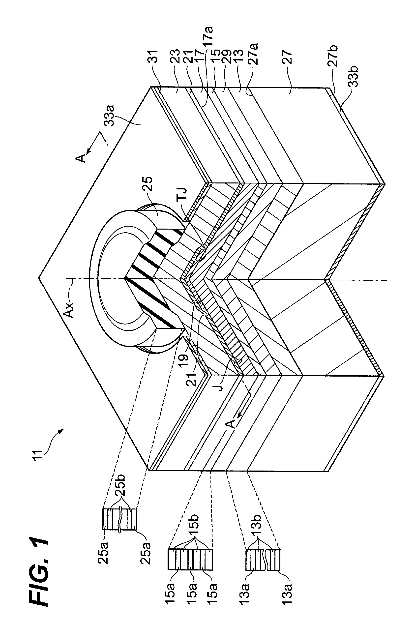
[0021]FIG. 1 is a perspective drawing of a vertical cavity surface emitting layer diode (VCSEL) according to an embodiment of the present invention. The VCSEL 11 provides a first Bragg reflector (hereafter denoted as the first DBR) 13, an active layer 15, a p-type space layer 17, a heavily doped p-type mesa 19, a heavily doped n-type layer 21, a first n-type space layer 23, and a second DBR layer (hereafter denoted as the second DBR) 25. FIG. 2A is a cross section of the VCSEL shown in FIG. 1, which is taken along the line A-A. The arrangement of ...


PUM


Abstract

A VCSEL with a structure able to reduce the scattering within the optical cavity and its manufacturing method are disclosed. The VCSEL of the present invention provides, on the semiconductor substrate, the first DBR, the active layer, the p-type spacer layer, the heavily doped p-type mesa, the heavily doped n-type layer, the first n-type spacer and the second DBR in this order. The heavily doped n-type layer, which is formed so as to cover the p-type spacer layer and the heavily doped p-type mesa, forms the tunnel junction with respect to the heavily doped p-type mesa. Because the height, which is appeared in the surface of the n-type spacer layer, reflects the height of the heavily doped p-type mesa and is comparatively small, the light scattering between the second DBR and the n-type spacer layer is suppressed.

Description

BACKGROUND OF THE INVENTION[0001]1. Field of the Invention[0002]The present invention relates to a vertical cavity surface emitting laser diode (hereafter simply denoted as VCSEL) and a method to form the VCSEL.[0003]2. Relater Background Art[0004]Nishiyama et al. has reported one type VCSEL in Electronics Letters, vol. 39 (5) (2003) pp. 437-439, in which the VCSEL provides, on the InP substrate, a Bragg reflector (hereafter simply denoted as DBR) formed by a combination of AlGaInAs and InP, an active layer, an n-type InP layer to bury a tunnel junction region with a mesa shape, and another Bragg reflector (DBR) made of multi-layered dielectric film. The mesa shaped tunnel junction region is formed by an etching of a heavily doped p-type layer and a heavily doped n-type layer.[0005]The VCSEL described above provides the mesa shaped tunnel junction region after the formation of double layers of the heavily doped n-type and p-type layers; accordingly, the height of the mesa for the tu...

Claims


Application Information

Patent Timeline
IPC IPC(8): H01S5/125H01L21/20
CPCH01S5/0421H01S5/3095H01S5/18369H01S5/18308
Inventor ONISHI, YUTAKA
Owner SUMITOMO ELECTRIC IND LTD
Why Eureka
Try Eureka