Organic light emitting diode and method of fabricating the same
- Summary
- Abstract
- Description
- Claims
- Application Information
AI Technical Summary
Benefits of technology
Problems solved by technology
Method used
Image

Examples
experimental example
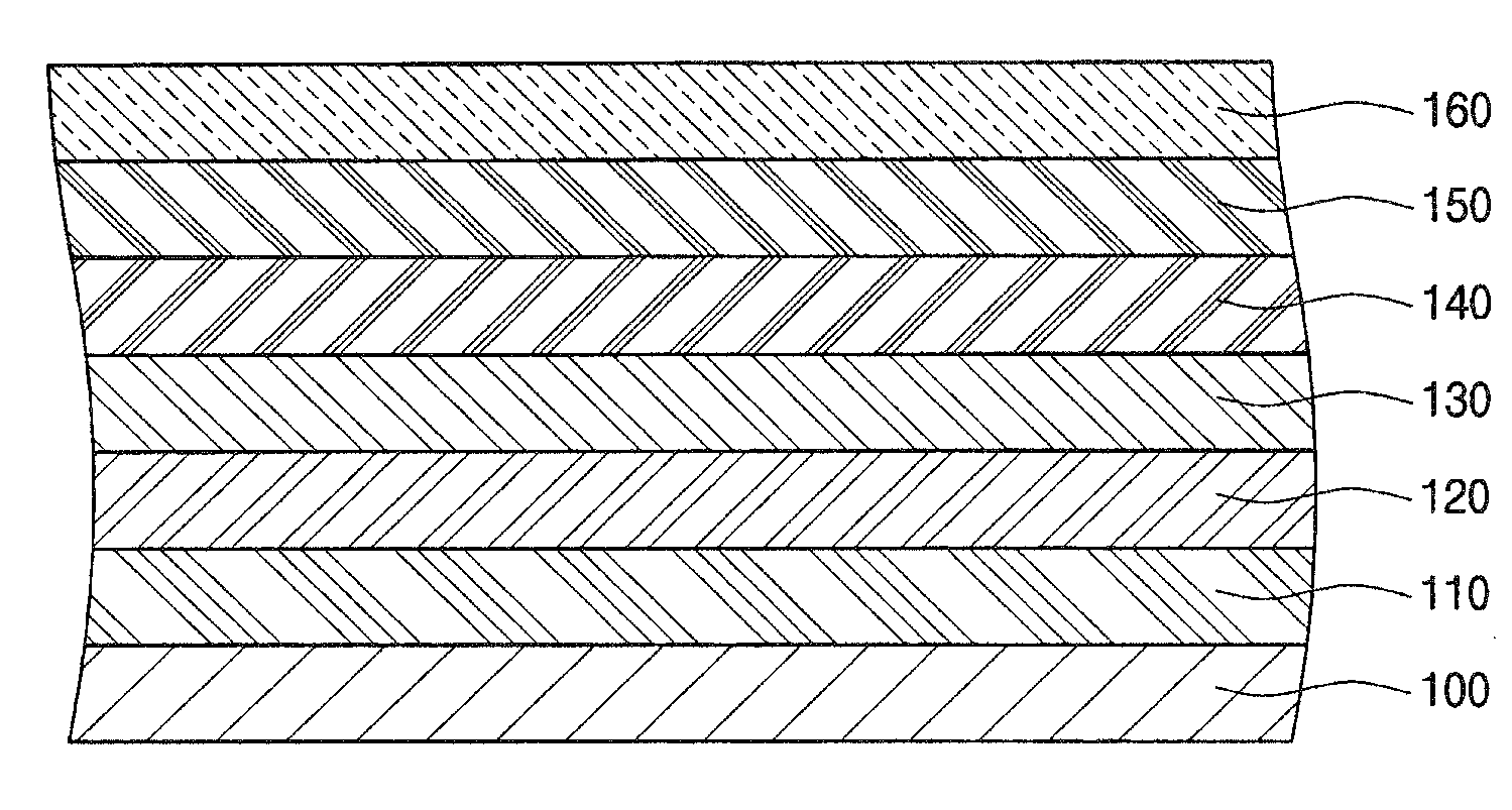
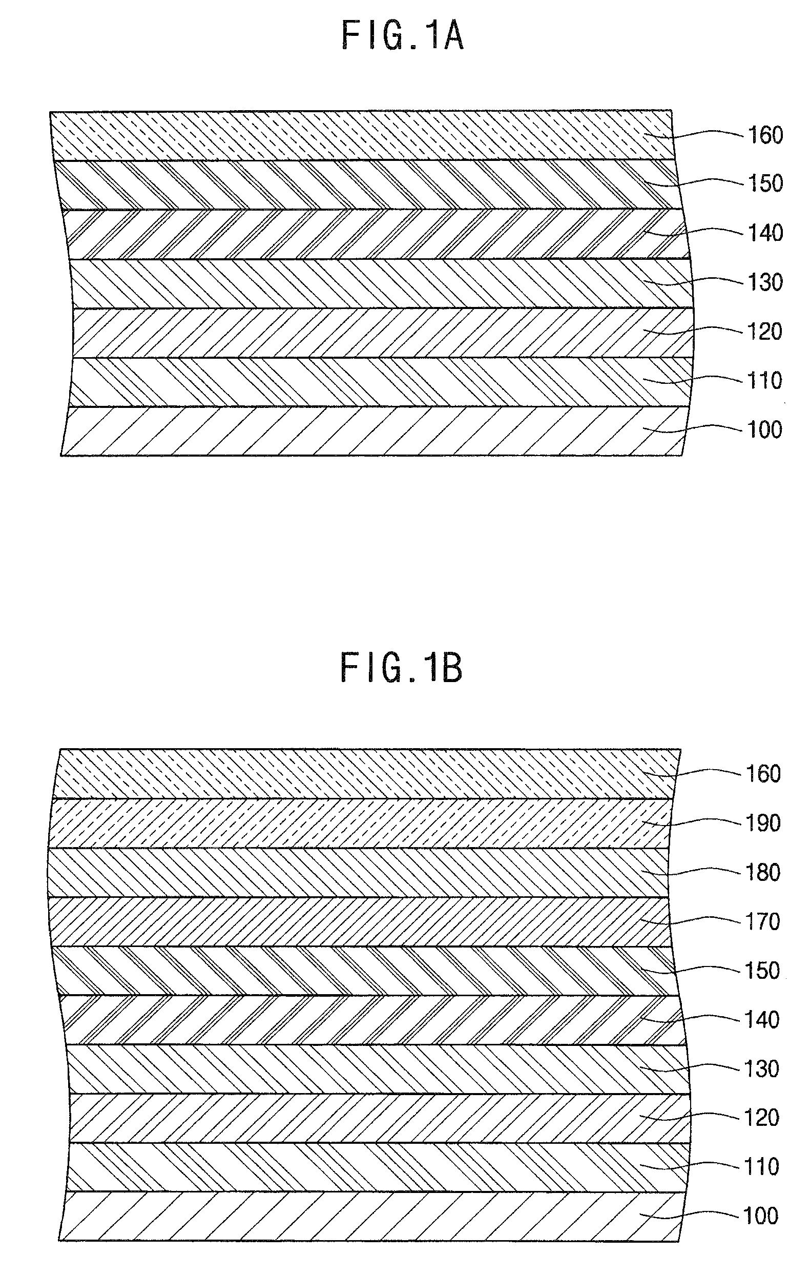
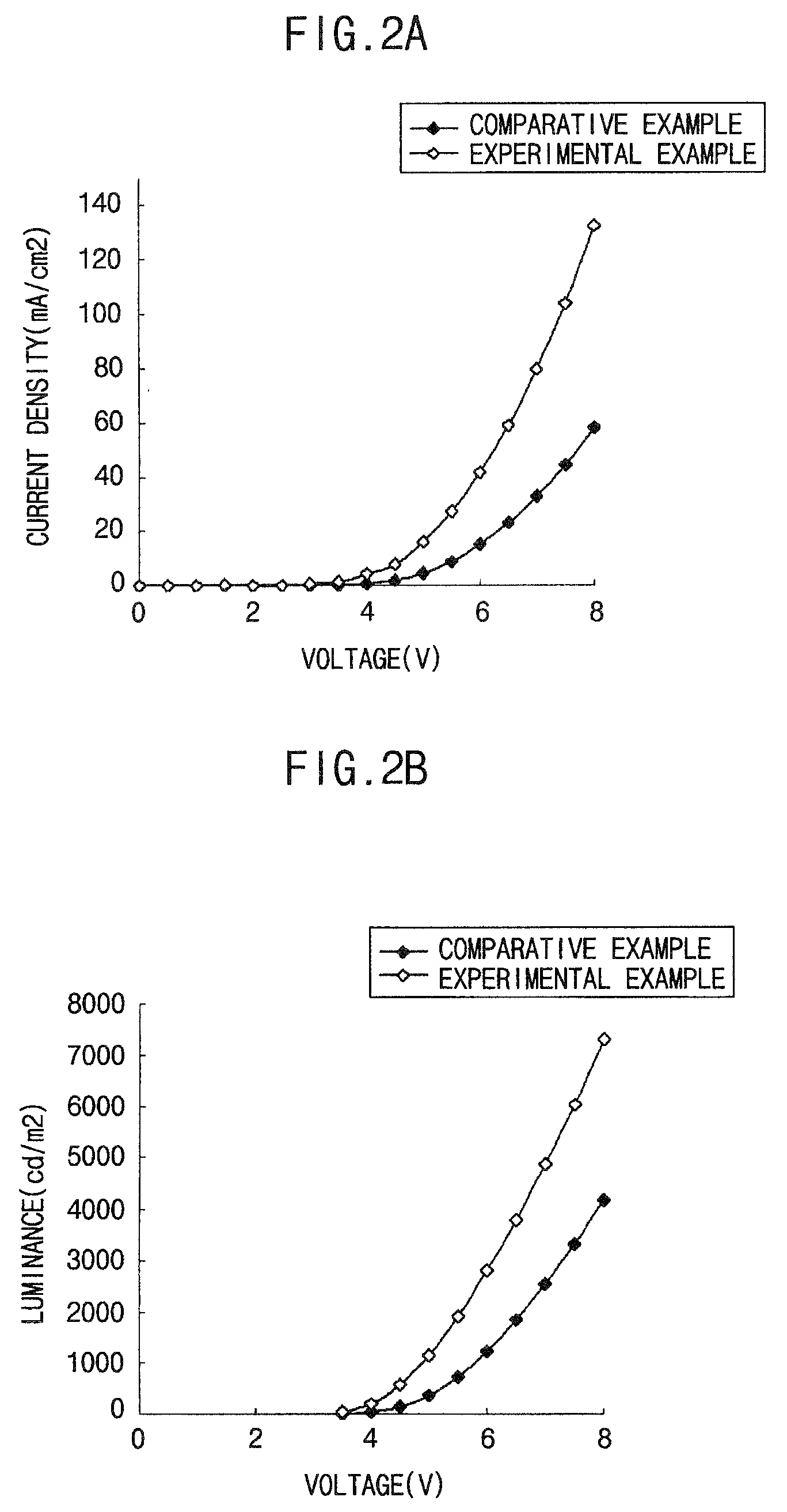
[0039]A first electrode was formed of ITO to a thickness of about 1000 Å. Thereafter, a hole injection layer was formed of mTDATA on the first electrode to a thickness of about 600 Å, and a first hole transport layer was formed of NPB on the hole injection layer to a thickness of about 150 Å. An intermediate layer was formed of MoO3 on the first hole transport layer to a thickness of about 50 Å. A second hole transport layer was formed of NPB on the intermediate layer to a thickness of about 100 Å. A red phosphorescent emission layer was formed on the second hole transport layer utilizing a mixture of CBP, as a host, and 12% by weight of Ir(piq)3, as a dopant, to a thickness of about 300 Å. An electron transport layer was formed of Alq3 on the red phosphorescent emission layer to a thickness of about 350 Å. Subsequently, an electron injection layer was formed of LiF on the electron transport layer to a thickness of about 5 Å. A second electrode was formed of Al on the electron injec...
PUM
 Abstract
Description
Claims
Application Information
 - R&D
- Intellectual Property
- Life Sciences
- Materials
- Tech Scout
- Unparalleled Data Quality
- Higher Quality Content
- 60% Fewer Hallucinations
Browse by: Latest US Patents, China's latest patents, Technical Efficacy Thesaurus, Application Domain, Technology Topic, Popular Technical Reports.
© 2025 PatSnap. All rights reserved.Legal|Privacy policy|Modern Slavery Act Transparency Statement|Sitemap|About US| Contact US: help@patsnap.com