Stacked solid electrolytic capacitor
a technology of electrolytic capacitors and stacking, which is applied in the direction of fixed capacitor details, variable capacitors, fixed capacitors, etc., can solve the problem that stacking advantages cannot be exploited
- Summary
- Abstract
- Description
- Claims
- Application Information
AI Technical Summary
Benefits of technology
Problems solved by technology
Method used
Image
Examples
example 1
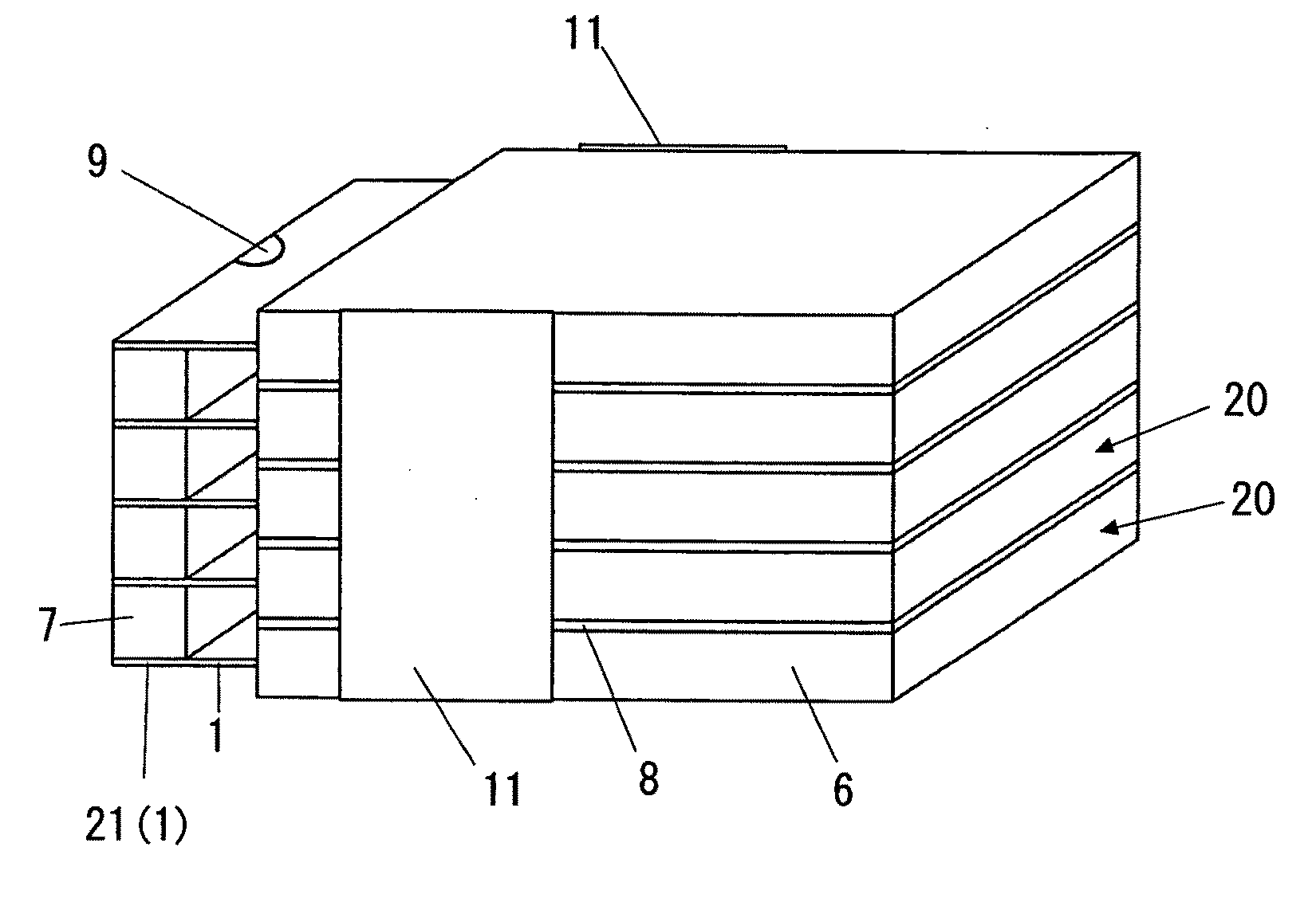
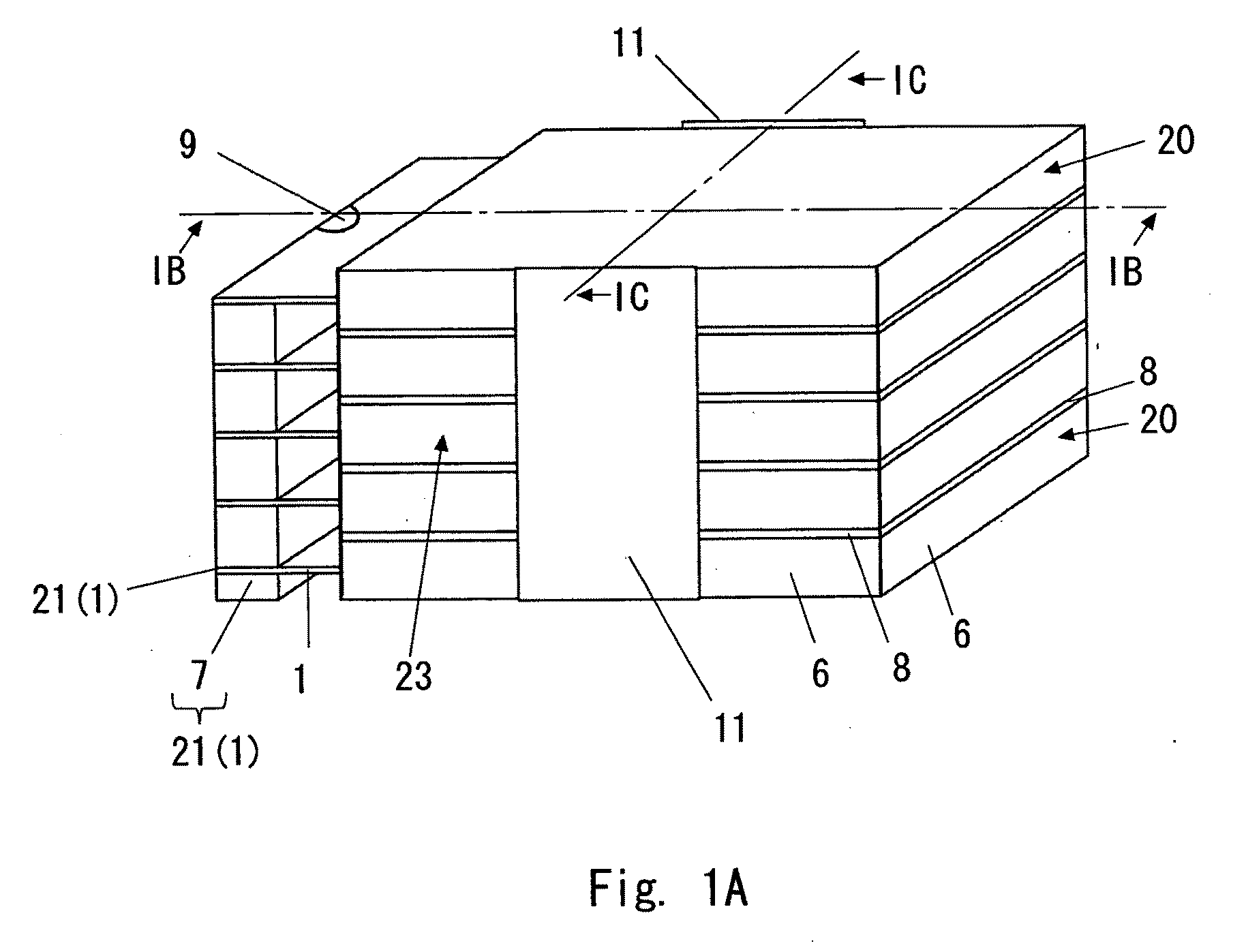
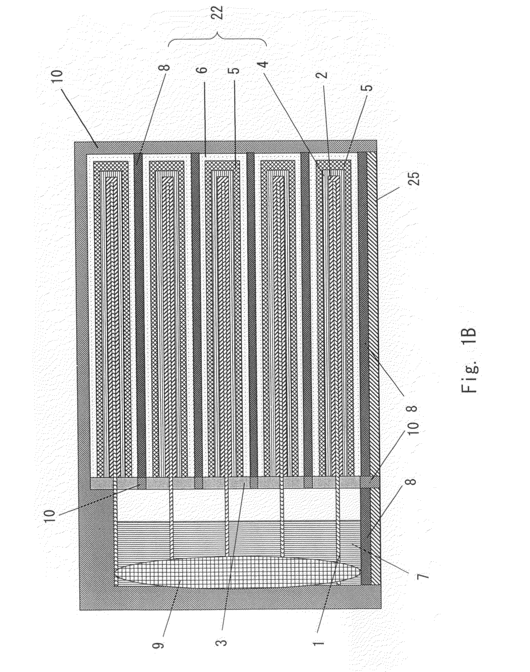
[0038]FIG. 1A is a perspective-view diagram of a stacked solid electrolytic capacitor according to Example 1 of the present invention, prior to encapsulation. FIG. 1B is a cross-sectional diagram, corresponding to a section IB-IB in FIG. 1A, of the stacked solid electrolytic capacitor according to Example 1 of the present invention, after encapsulation. Similarly, FIG. 1C is a cross-sectional diagram, corresponding to a section IC-IC in FIG. 1A, of the stacked solid electrolytic capacitor according to Example 1, after encapsulation. Firstly, an anode body 1 (valve action metal) comprising a surface-roughened flat aluminum foil was anodized, to form thereby a dielectric 2 having formed thereon an anodized film. Then there was formed a resist layer 3 for isolating a cathode section from the end of the anode, not surface-roughened, that yields the anode section. A solid electrolyte 4, comprising a conductive polymer, was formed then on the dielectric 2, followed by formation of graphit...
example 2
[0044]A stacked aluminum solid electrolytic capacitor was manufactured in the same way as in Example 1, but forming the solid electrolyte using manganese dioxide instead of the conductive polymer used in Example 1.
example 3
[0049]A 5-layer stack was manufactured after forming aluminum solid electrolytic capacitor elements as in Example 1. Thereafter, parts of the anode sections of the aluminum solid electrolytic capacitor elements were connected by laser welding, to form an anode laser welded section. Thereafter, stacked aluminum solid electrolytic capacitors were manufactured using a silver paste (Example 3a), a copper paste (Example 3b), or a paste comprising a 1:1 mixture of a silver filler and a copper filler (Example 3c), as the conductive layers formed on the central portion of the side faces of the stacked cathode layers.
PUM
| Property | Measurement | Unit |
|---|---|---|
| area | aaaaa | aaaaa |
| conductive | aaaaa | aaaaa |
| surface area | aaaaa | aaaaa |
Abstract
Description
Claims
Application Information
 - R&D
- Intellectual Property
- Life Sciences
- Materials
- Tech Scout
- Unparalleled Data Quality
- Higher Quality Content
- 60% Fewer Hallucinations
Browse by: Latest US Patents, China's latest patents, Technical Efficacy Thesaurus, Application Domain, Technology Topic, Popular Technical Reports.
© 2025 PatSnap. All rights reserved.Legal|Privacy policy|Modern Slavery Act Transparency Statement|Sitemap|About US| Contact US: help@patsnap.com


