Micro-electro-mechanical systems (MEMS) device and process for fabricating the same
- Summary
- Abstract
- Description
- Claims
- Application Information
AI Technical Summary
Benefits of technology
Problems solved by technology
Method used
Image

Examples
Embodiment Construction
[0068]The present invention provides novel MEMS structures. This invention is directed to the integration of a MEMS device and CMOS devices by taking advantage of semiconductor fabrication process. In such technology, a MEMS device with a low cost for fabrication, a miniature size and high performance for application can be obtained. Moreover, for example, the present invention takes a few process steps to accomplish the integration of MEMS devices in addition to the CMOS process. The invention can be implemented on many MEMS devices, such as MEMS microphone, MEMS speaker or pressure sensor that needs a flexible diaphragm as a capacitive sensor; or accelerometer, switches or variable capacitor that needs various designed.
[0069]Several embodiments are provided for descriptions but not for limiting the present invention. Also noted, the disclosure in different embodiments may be properly combined as another embodiment.
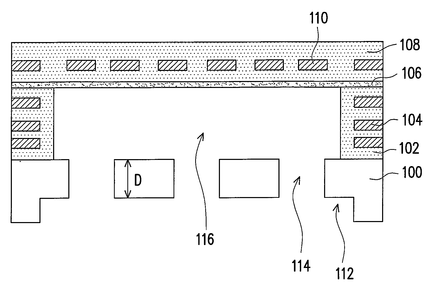
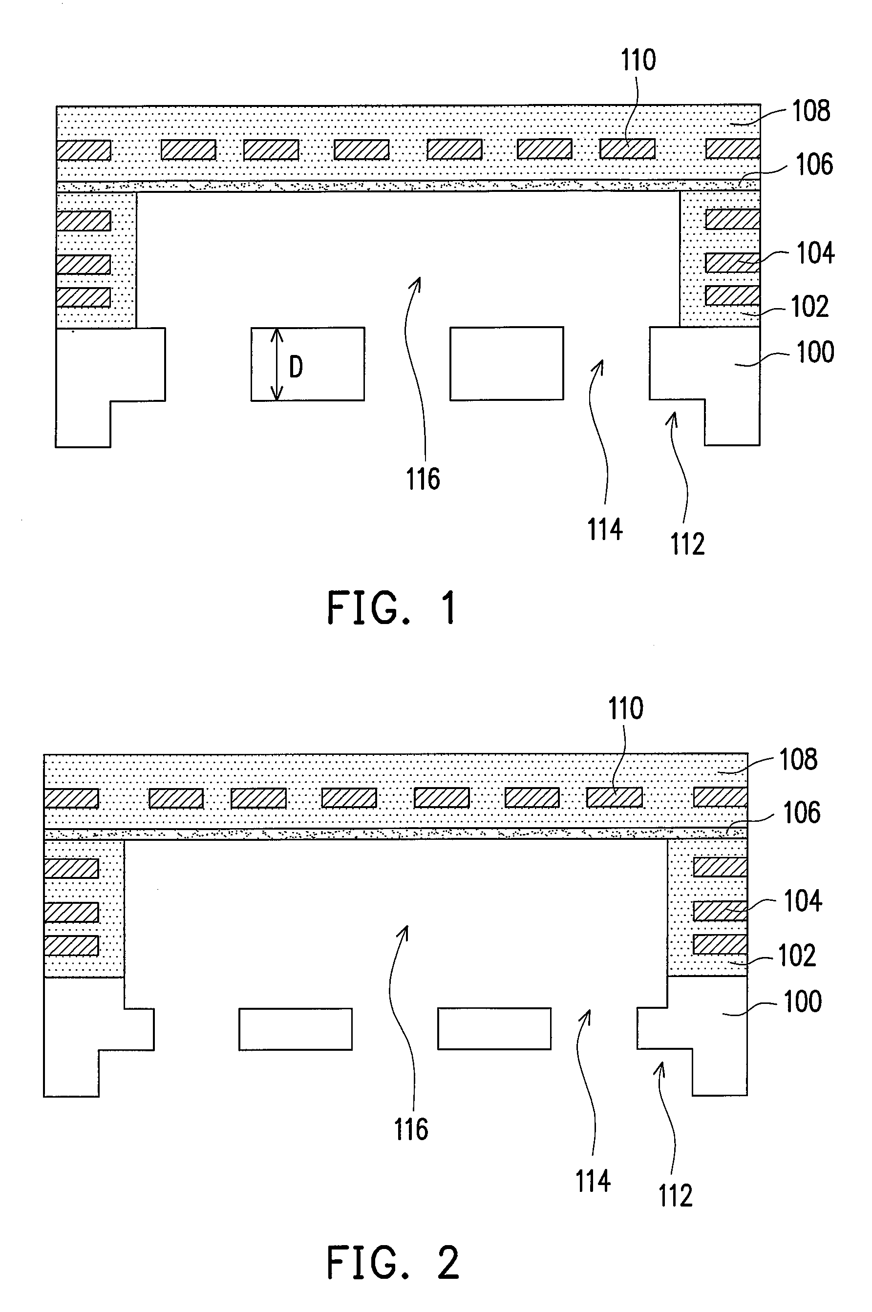
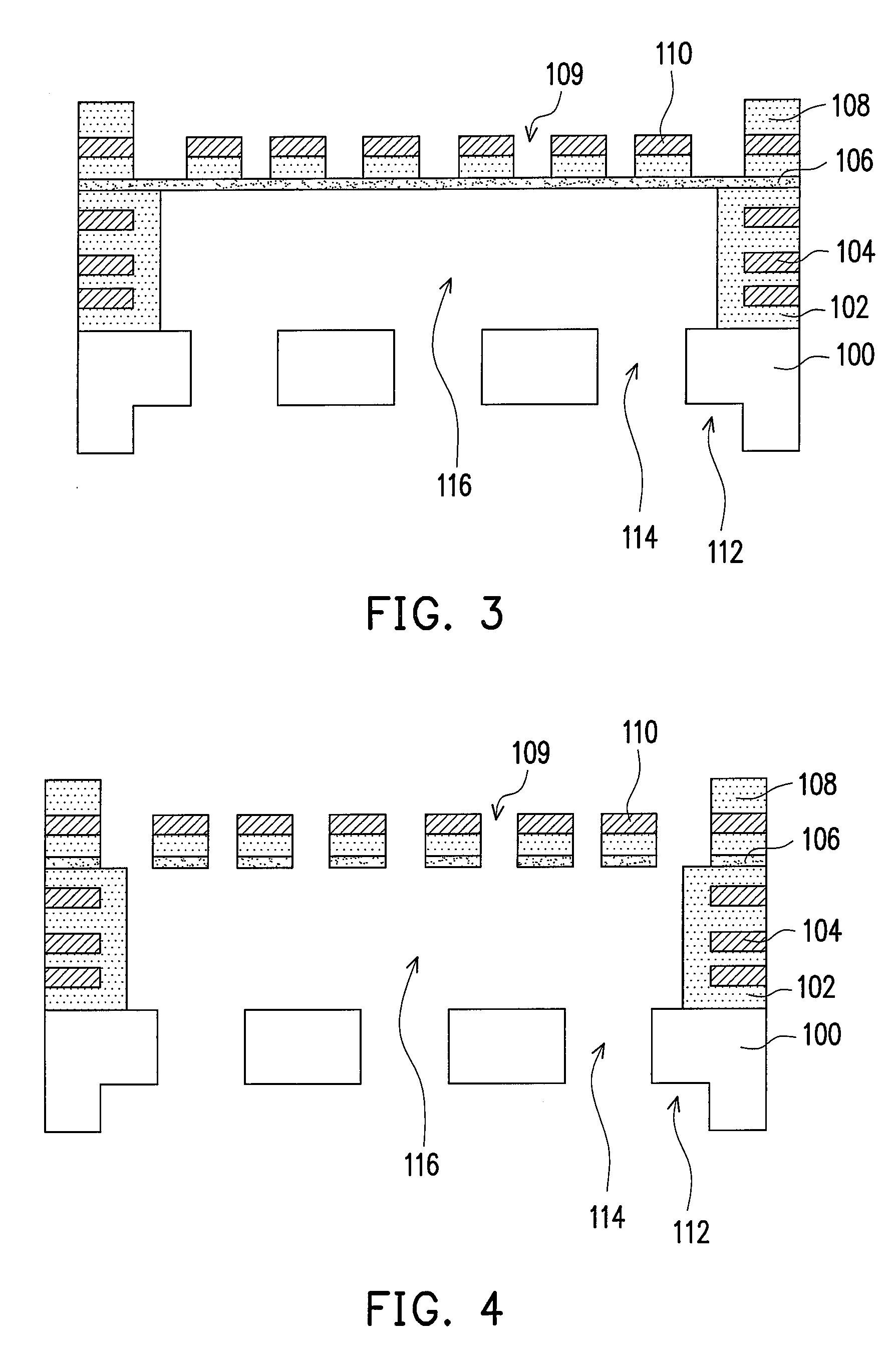
[0070]FIG. 1 is a cross-sectional view, schematically illustrating ...
PUM
| Property | Measurement | Unit |
|---|---|---|
| Dielectric polarization enthalpy | aaaaa | aaaaa |
| Angle | aaaaa | aaaaa |
| Shape | aaaaa | aaaaa |
Abstract
Description
Claims
Application Information
 - R&D
- Intellectual Property
- Life Sciences
- Materials
- Tech Scout
- Unparalleled Data Quality
- Higher Quality Content
- 60% Fewer Hallucinations
Browse by: Latest US Patents, China's latest patents, Technical Efficacy Thesaurus, Application Domain, Technology Topic, Popular Technical Reports.
© 2025 PatSnap. All rights reserved.Legal|Privacy policy|Modern Slavery Act Transparency Statement|Sitemap|About US| Contact US: help@patsnap.com