
Semiconductor apparatus

a technology of semiconductor elements and apparatuses, applied in the direction of electrical apparatus, semiconductor devices, semiconductor/solid-state device details, etc., can solve the problems of thermal stress, semiconductor element breakage, electrical characteristics may become inappropriate, etc., to prevent the breakage of semiconductor elements, reduce stress, and reduce stress induced

Inactive Publication Date: 2009-05-28
ELPIDA MEMORY INC
View PDF4 Cites 64 Cited by
  • Summary
  • Abstract
  • Description
  • Claims
  • Application Information

AI Technical Summary

Benefits of technology

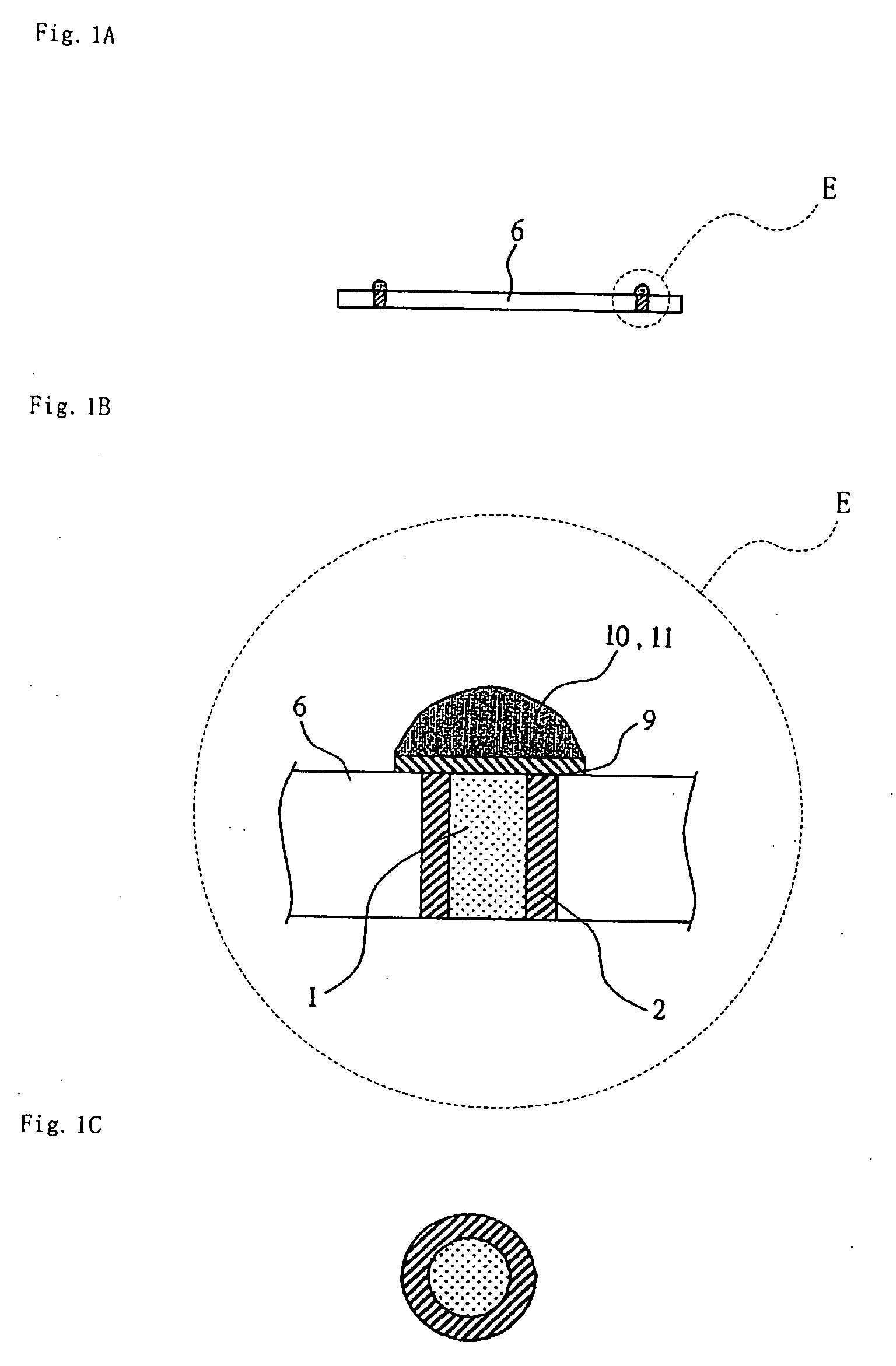
[0010]the electrode is formed as a cylinder including a hollow portion, and stress relaxing material is provided in the hollow portion, which is used to reduce stress induced between the semiconductor element and the electrode. The following materials are, for example, used as the stress relaxing material: a low-elastic body which is made of photosensitive resin, and whose elasticity is relatively small, SiO2, polysilicon, conductive paste, and the like.
[0011]According to the present invention, it is possible to reduce stress induced around the electrode provided in the semiconductor element, and to prevent the semiconductor element from being broken as a result of a crack being induced in the semiconductor element, and to prevent inappropriate electric characteristics from being induced.

Problems solved by technology

However, when Cu is used as material of the through electrode, it is concerned that thermal stress is induced because of the difference of the thermal expansion ratio between silicon configured in the semiconductor element and Cu (thermal expansion ratio of Cu: around 17 ppm / K, thermal expansion ratio of silicon: around 3 ppm / K).
In particular, when the semiconductor element is connected to another electronic element or a board, the semiconductor element is normally heated up to nearly 300° C. In this case, large stress is induced around the electrode, a crack is induced in the silicon configured in the semiconductor element, as a result of which the semiconductor element may be broken.
The large stress is induced around the electrode because the temperature is elevated when the semiconductor element is used, the electric characteristics are changed because of the induced stress, and the electric characteristics may become inappropriate.

Method used


Image

  • Semiconductor apparatus
  • Semiconductor apparatus
  • Semiconductor apparatus

Examples


first exemplary embodiment

[0045]The semiconductor apparatus of a first exemplary embodiment will be described by referring to FIGS. 11A and 11B to FIG. 16.

[0046]FIG. 11A illustrates a cross-section view illustrating the electrode neighborhood of a chip of the semiconductor apparatus, and FIG. 11B illustrates a cross-section view obtained by cutting an A-B cutting line of FIG. 11A.

[0047]Referring now to FIG. 11A and FIG. 11B, the semiconductor apparatus of the present exemplary embodiment is provided with semiconductor element (chip) 6. This semiconductor element 6 is provided with cylindrical electrode 2 passing in a thickness direction through front and back sides of semiconductor element 6. Stress relaxing material 1 is provided in a hollow portion of this electrode 2. In semiconductor element 6, insulation layer 3 is formed as concentrically surrounding electrode 2 in an outer circle side of cylindrical electrode 2. The back side of semiconductor element 6 is, excluding electrode 2, covered with insulatio...

second exemplary embodiment

[0065]Referring to FIG. 17, the semiconductor apparatus of a second exemplary embodiment will now be described. FIG. 17 illustrates a cross-section view illustrating the electrode neighborhood of the semiconductor element included in the semiconductor apparatus of the present exemplary embodiment.

[0066]As illustrated in FIG. 17, a point of difference between the semiconductor element included in the semiconductor apparatus of the present exemplary embodiment and the semiconductor element included in the semiconductor apparatus of the first exemplary embodiment is that central axis C2 of connection pad 5, which is electrically connected to a connection bump of another semiconductor element stacked to the semiconductor element, is arranged at a position separated from central axis C1 of cylindrical electrode 2.

[0067]In this configuration, particularly, when the inside of the hollow portion of electrode 2 is filled with photosensitive resin used as stress relaxing material, a structure...

third exemplary embodiment

[0072]Referring to FIG. 18, the semiconductor apparatus of the present exemplary embodiment will be described. FIG. 18 illustrates a cross-section view around the electrode of the semiconductor element included in the semiconductor apparatus of the present exemplary embodiment.

[0073]The semiconductor element included in the semiconductor apparatus of the present exemplary embodiment is configured so that the inside of the hollow portion of electrode 2 is filled with photosensitive resin used as stress relaxing material 1, and the structure of the back side of semiconductor element 6 is different from that of the second exemplary embodiment.

[0074]That is, for the semiconductor element included in the semiconductor apparatus of the present exemplary embodiment, on the back side of semiconductor element 6, connection pad 5 is formed to be electrically connected to a part of the edge face of electrode 2 on the surface of electrode 2 which passes through the front and back sides of semic...


PUM


Abstract

The present invention includes a semiconductor element provided with an electrode passing through front and back sides. The electrode is formed as a cylinder including a hollow portion, and stress relaxing material is provided in the hollow portion, which is used to reduce stress that is induced between the semiconductor element and the electrode. The stress relaxing material is an elastic body made of resin material.

Description

BACKGROUND OF THE INVENTION[0001]1. Field of the Invention[0002]The present invention relates to a semiconductor apparatus, and particularly, to a semiconductor apparatus provided with a semiconductor element including an electrode (through electrode) which is provided to pass through the semiconductor element (chip).[0003]2. Description of the Related Art[0004]In recent years, a semiconductor apparatus is required to achieve further high-performance and downsizing.[0005]In response to this request, such a configuration, wherein a through electrode is formed in a semiconductor element, and a plurality of the semiconductor elements are stacked to be connected to each other by using a bump connected to the through electrode, is focused on. Such a configuration is disclosed in the following documents, for example, Japanese Patent Laid-Open No. 10-223833; Japanese Patent Laid-Open No. 2004-152810; and Non-Patent Document (Japan Institute of Electronics Packaging Journal, Vol. 7, No. 1 (...

Claims


Application Information

Patent Timeline
IPC IPC(8): H01L23/538H01L23/52H01L23/58
CPCH01L21/76898H01L23/3128H01L2924/01033H01L2924/01024H01L2924/01019H01L2924/01006H01L2924/00013H01L2924/15311H01L2924/014H01L23/481H01L24/02H01L24/11H01L24/12H01L25/0657H01L25/50H01L2224/0401H01L2224/1308H01L2224/13082H01L2224/13111H01L2224/13147H01L2224/16H01L2224/2518H01L2225/06513H01L2225/06541H01L2924/01004H01L2924/01005H01L2924/01014H01L2924/01022H01L2924/01028H01L2924/01029H01L2924/0105H01L2924/01051H01L2924/01082H01L2924/00014H01L2224/13099H01L2924/351H01L24/05H01L24/13H01L2224/0557H01L2224/13025H01L2224/023H01L2924/00H01L2924/0001
Inventor IKEDA, HIROAKIISHINO, MASAKAZUMIYAKE, HIDEHARUUCHIYAMA, SHIRONAKA, YASUHIROHISANO, NAETANIE, HISASHINISHI, KUNIHIKOTENMEI, HIROYUKI
Owner ELPIDA MEMORY INC
Learn More