Phase change memory cell including a thermal protect bottom electrode and manufacturing methods

Active Publication Date: 2009-05-14
MACRONIX INT CO LTD
View PDF99 Cites 26 Cited by
  • Summary
  • Abstract
  • Description
  • Claims
  • Application Information

AI Technical Summary

Benefits of technology

[0013]In memory cells described herein the active region can be made extremely small, reducing the magnitude of current needed to induce phase changes. In preferred embodiments the width (which in some embodiments is a diameter) of the phase change kernel is less than a minimum feature size for a lithographic process used to form the memory cell. The thickness of the kernel can also be less than the minimum feature size for a lithographic process used to form the memory cell, and the thickness can be established by a thin film deposition technique of memory material on the thermal protect structure.

Problems solved by technology

Deposited material tends to cling to the sides of a receptacle structure, leaving voids or seams instead of a uniformly solid material.
Because of its high conformity, tungsten is particularly susceptible to that phenomenon.
In such an instance, the subsequently deposited phase change kernel 120 may not make full contact with the bottom electrode 110, resulting in a poor contact and issues with memory cell stability and reliability.
Problems have arisen in manufacturing such devices with very small dimensions, and with variations in processes that meet the tight specifications needed for large-scale memory devices.

Method used


Image

  • Phase change memory cell including a thermal protect bottom electrode and manufacturing methods
  • Phase change memory cell including a thermal protect bottom electrode and manufacturing methods
  • Phase change memory cell including a thermal protect bottom electrode and manufacturing methods

Examples


first embodiment

[0058]FIGS. 6-12 illustrate an embodiment of a process flow for manufacturing a memory cell in accordance with a The following description does not repeat certain explanations regarding materials, thicknesses, and the like, as set out above.

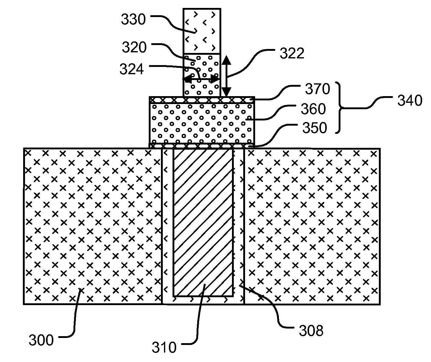
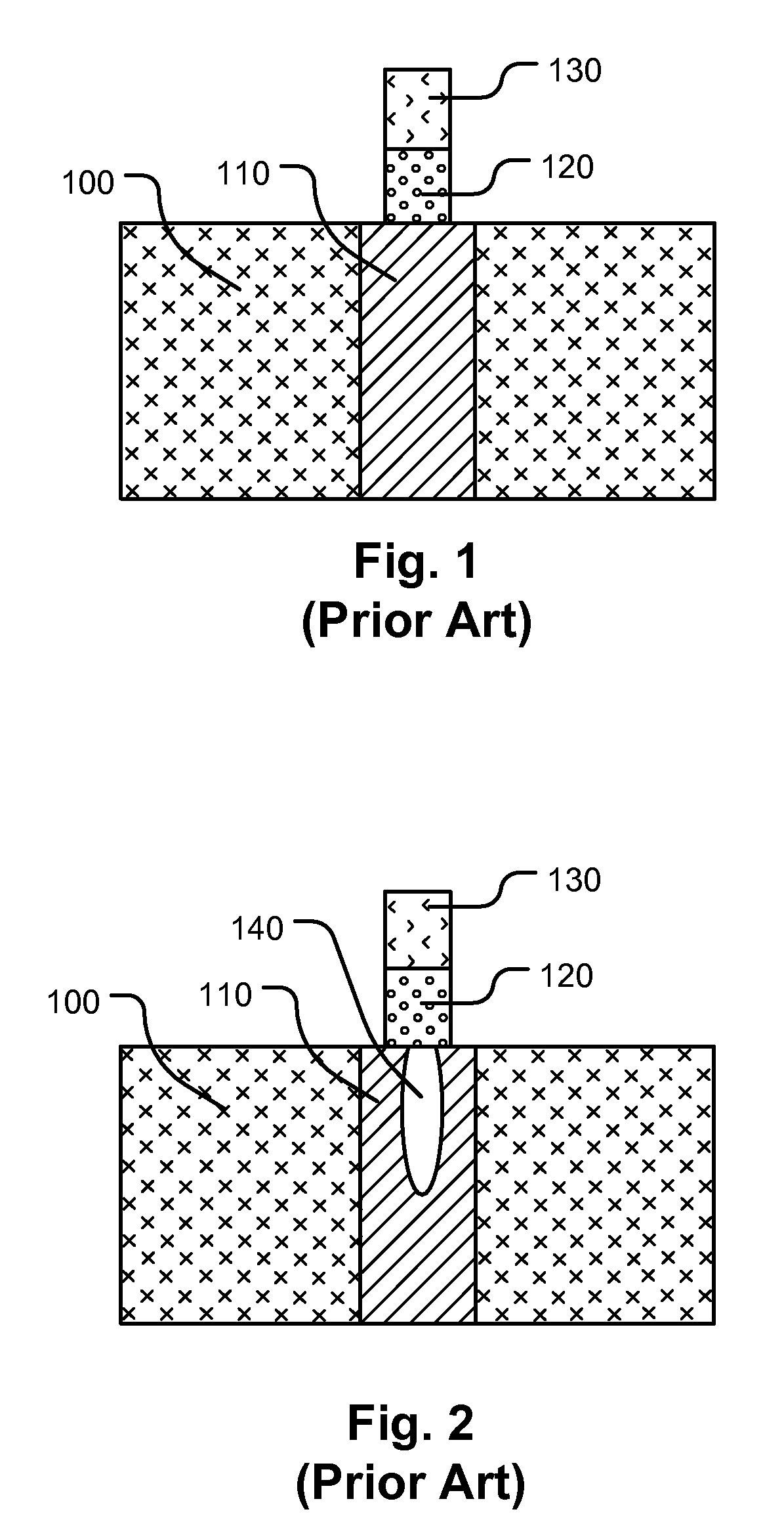
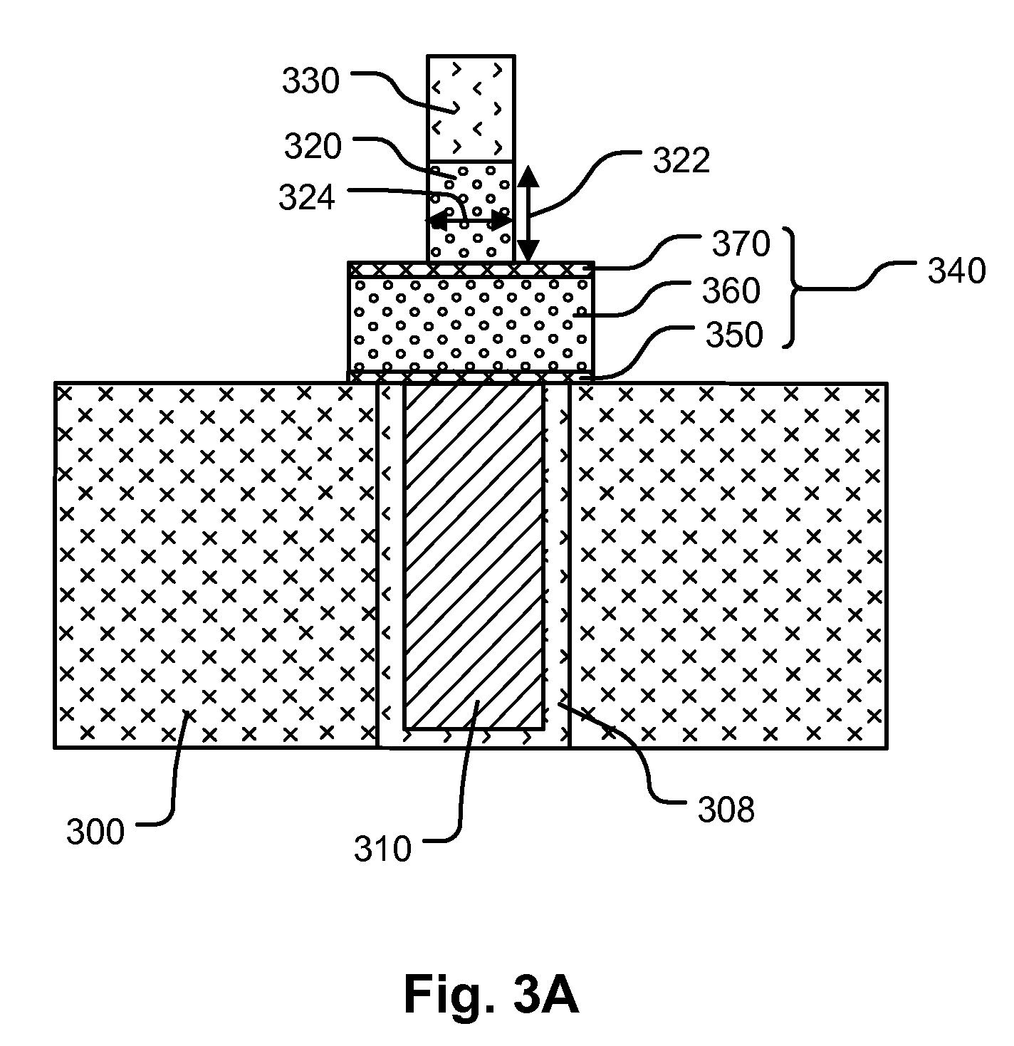
[0059]FIG. 6 illustrates a cross-sectional view of a first step in a process flow comprising providing an inter-layer dielectric 300 having a bottom electrode (contact) 310 extending therethrough.

[0060]Next, a multi-layer structure is formed on the structure illustrated in FIG. 6 comprising sequentially forming a layer of first barrier material 750, a layer of thermal protect material 760, a layer of second barrier material 770, a layer of phase change material 720, a layer of top electrode material 730, and a layer of hard mask material 700, resulting in the structure illustrated in FIG. 7. The hard mask material 700 in some embodiments comprises SiN, SiO2, or SiON.

[0061]Next, a pillar 800 comprising photoresist material is formed on the struct...

second embodiment

[0066]FIGS. 13-20 illustrate an embodiment of a process flow for manufacturing a memory cell in accordance with a

[0067]FIG. 13 illustrates a cross-sectional view of a process flow comprising providing an inter-layer dielectric 500 having a bottom electrode 510 extending therethrough.

[0068]Next, a portion of the bottom electrode 510 illustrated in FIG. 13 is etched to form a recess 1400, resulting in the structure illustrated in FIG. 14.

[0069]Next, a conformal layer a first barrier material 1500 is formed on the structure illustrated in FIG. 14, resulting in the structure illustrated in FIG. 15. The first barrier material 1500 within the recess defines an opening 1510 within the recess 1400.

[0070]A layer of thermal protect material is formed on the structure illustrated in FIG. 15 and then a planarizing process such as Chemical Mechanical Polishing CMP is performed, resulting in the structure illustrated in FIG. 15 having a first barrier layer 550 and a thermal protect layer 560 form...


PUM

PropertyMeasurementUnit
Fractionaaaaaaaaaa
Fractionaaaaaaaaaa
Electrical conductivityaaaaaaaaaa

Abstract

Memory devices are described along with manufacturing methods. An embodiment of a memory device as described herein includes a bottom electrode, a thermal protect structure on the bottom electrode, and a multi-layer stack on the thermal protect structure. The thermal protect structure comprises a layer of thermal protect material, the thermal protect material having a thermal conductivity less than that of the bottom electrode material.

Description

BACKGROUND OF THE INVENTION[0001]1. Field of the Invention[0002]The present invention relates to high density memory devices based on phase change based memory materials, including chalcogenide based materials and on other programmable resistive materials, and to methods for manufacturing such devices.[0003]2. Description of Related Art[0004]Phase change based memory materials are widely used in read-write optical disks. These materials have at least two solid phases, including for example a generally amorphous solid phase and a generally crystalline solid phase. Laser pulses are used in read-write optical disks to switch between phases and to read the optical properties of the material after the phase change.[0005]Phase change based memory materials, like chalcogenide based materials and similar materials, also can be caused to change phase by application of electrical current at levels suitable for implementation in integrated circuits. The generally amorphous state is characteriz...

Claims


Application Information

Patent Timeline
IPC IPC(8): G11C5/00B05D5/12C23F1/02
CPCH01L45/06H01L45/1233H01L45/1293H01L45/143H01L45/1675H01L45/148H01L45/1625H01L45/1641H01L45/144H10N70/231H10N70/8616H10N70/8825H10N70/826H10N70/884H10N70/8828H10N70/026H10N70/041H10N70/063
Inventor CHEN, SHIH HUNG
Owner MACRONIX INT CO LTD
Why Eureka
Try Eureka