Indene derivative compound and organic light emitting device comprising the same

Active Publication Date: 2009-04-16
SAMSUNG DISPLAY CO LTD
View PDF4 Cites 13 Cited by
  • Summary
  • Abstract
  • Description
  • Claims
  • Application Information

AI Technical Summary

Benefits of technology

[0011]The present invention provides an indene derivative compound capable of improving driving voltage properties, efficiency and color purity of an organic light emitting device and an organic light emitting device including the indene derivative compound.
[0019]An organic light emitting device prepared using an indene derivative compound represented by Formula 1 according to the present invention can have improved emitting properties such as excellent driving voltage properties, high efficiency, high brightness and high color purity by forming a thermally stable organic layer.

Problems solved by technology

However, the organic light emitting device including the anthracene does not have sufficient driving voltage, brightness, efficiency and color purity properties, and thus those properties need to be improved.

Method used


Image

  • Indene derivative compound and organic light emitting device comprising the same
  • Indene derivative compound and organic light emitting device comprising the same
  • Indene derivative compound and organic light emitting device comprising the same

Examples


synthesis example 1

[0087]Compound 3 was synthesized through Reaction Scheme 1 below.

[0088]Synthesis of Intermediate A

Synthesis of 4,4,5,5-Tetramethyl-2-[4-(10-phenyl-anthracen-9-yl)-phenyl]-[1,3,2]dioxaborolane (a)

[0089]4.6 g (11.2 mmol) of 9-(4-Bromo-phenyl)-10-phenyl-anthracene was dissolved in 150 ml of THF in a 500 ml round-bottom flask in an argon atmosphere, and 6.36 ml (15.9 mmol) of 2.5 M n-BuLi (in hexane) was added thereto at −78° C. Then, the flask was stirred at −78° C. for 1 hour and 3.52 ml (17.23 mmol) of 2-isopropoxy-4,4,5,5-tetramethyl-1,3,2-dioxabororane was added thereto, and then the flask was stirred at room temperature for 2 hours. 50 ml of water was added to the flask to terminate the reaction, and the mixture was subject to extraction using brine and methylene chloride. The extracted organic layer was dried using anhydrous magnesium sulfate, filtered, and the solvent was removed. The resultant was dissolved in a small amount of toluene, impurities were removed by column chromat...

example 1

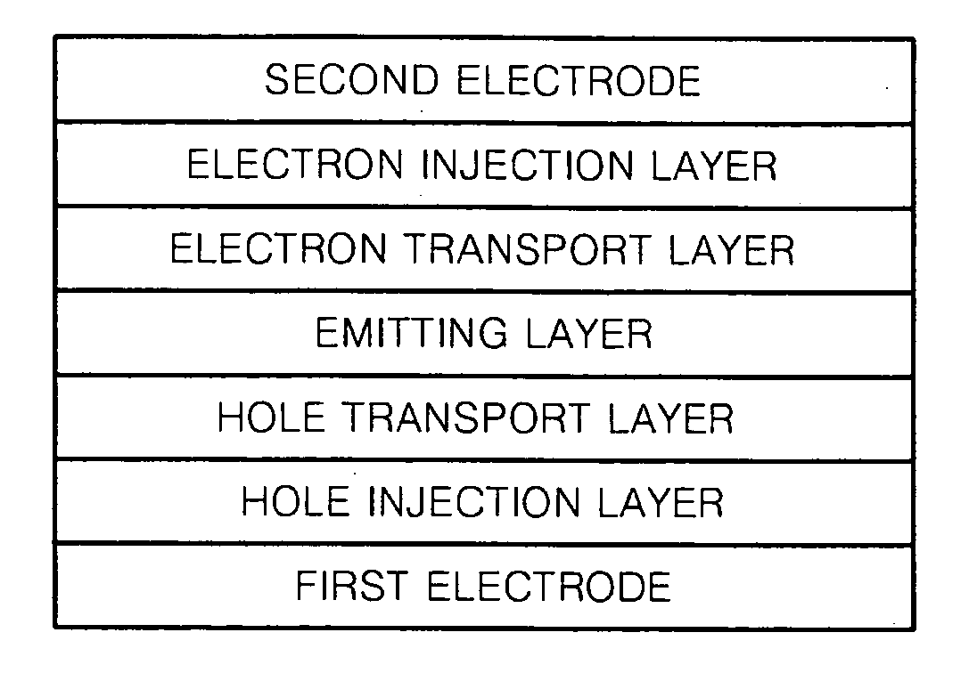
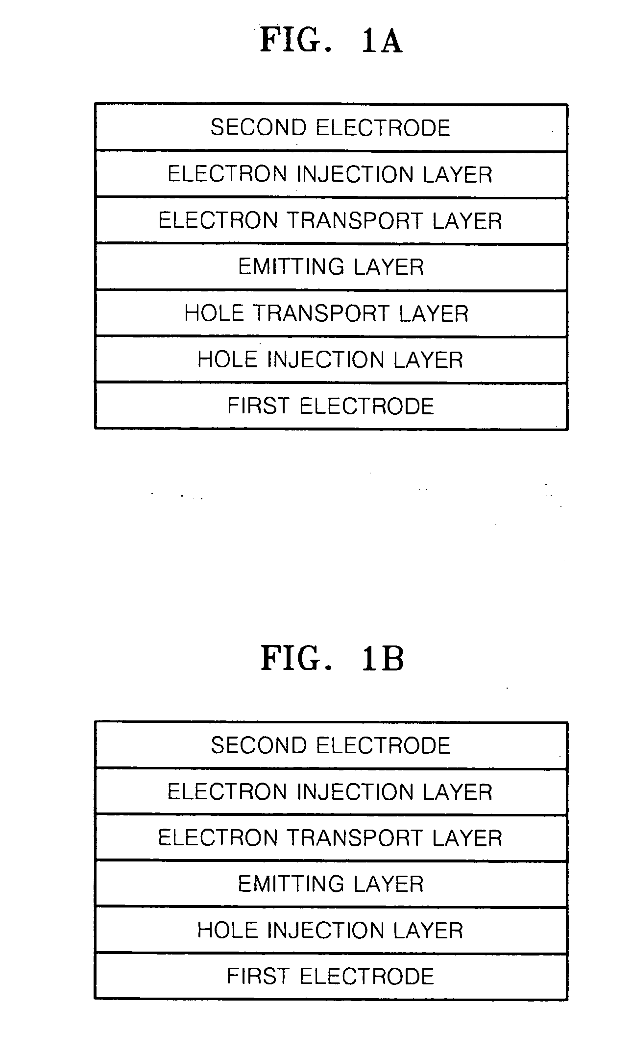
[0098]An organic light emitting device having a structure of ITO(1000 Å) / (M-TDATA) (35 nm) / α-NPD(30 nm) / (95% by weight of the compound of the present invention / 5% by weight of DPAVBi)(35 nm) / ALq3(18 nm) / LiF(0.7 nm) / Al(150 nm) was prepared using the synthesized Compound as a host and DPAVBi as a dopant of an emitting layer.

[0099]15 Ω / cm2 (1000 Å) ITO glass substrate was cut into pieces into 50 mm×50 mm×0.7 mm in size, followed by ultrasonic cleaning in isopropyl alcohol and deionized water for 15 minutes for each and then UV ozone cleaned for 30 minutes to produce an anode. M-TDATA was deposited on the substrate to a thickness of 35 nm, and α-NPD was vacuum deposited thereon to a thickness of 30 nm. Then, the compound according to the present invention and DPAVBi were vacuum deposited at the same time in a weight ratio of 95:5 to form an emitting layer with a thickness of 35 nm. Then, ALq3 was vacuum deposited on the emitting layer to form an electron transport layer with a thickness...


PUM

PropertyMeasurementUnit
Timeaaaaaaaaaa
Electric potential / voltageaaaaaaaaaa
Fluorescenceaaaaaaaaaa

Abstract

Provided are an indene derivative compound represented by Formula 1 below and an organic light emitting device including the same:X—Ar1—Ar2—Y   Formula 1wherein Ar1, Ar2 and X are described in the detailed description, andY is represented by one of Formulae 2a to 2d:wherein R1 to R4 and Z are described in the detailed description.An organic light emitting device having improved driving voltage properties, brightness, efficiency and color purity can be prepared by including the indene derivative compound.

Description

CLAIM OF PRIORITY[0001]This application makes reference to, incorporates the same herein, and claims all benefits accruing under 35 U.S.C. §119 from an application for earlier filed in the Korean Intellectual Property Office on 15 Oct. 2007 and there duly assigned Serial No. 10-2007-0103732.BACKGROUND OF THE INVENTION[0002]1. Field of the Invention[0003]The present invention relates to an indene derivative compound and an organic light emitting device including the same, and more particularly, to an indene derivative compound having excellent electrical properties and providing excellent driving voltage properties, high efficiency and high color purity to an organic light emitting device when applied to the organic light emitting device and an organic light emitting device including the indene derivative compound.[0004]2. Description of the Related Art[0005]Organic light emitting devices are active light emitting display devices that emit light by recombination of electrons and hole...

Claims


Application Information

Patent Timeline
IPC IPC(8): B32B15/04B32B9/04C07C49/67
CPCC07C49/67C07C13/465Y10T428/31678Y10T428/31504C09K11/06C07C13/66C07C13/54C09K2211/1011H10K85/622H10K85/615H10K50/00
Inventor KIM, MYEONG-SUKSHIN, DONG-WOOKIM, YU-JINCHOI, BYOUNG-KINOH, TAE-YONGKWON, O-HYUNLEE, TAE-WOOHAN, EUN-SILPAEK, WOON-JUNG
Owner SAMSUNG DISPLAY CO LTD
Why Eureka
Try Eureka