
Photovoltaic device and method of manufacturing the same

a photovoltaic and photovoltaic layer technology, applied in the field of photovoltaic devices, can solve the problems of affecting the environment when it is discarded, requiring a lot of energy during the process, and difficult to commercialize photovoltaic devices, and achieves the effect of preventing (or reducing) the deterioration of the electron conductivity of the surface-treated photovoltaic layer

Inactive Publication Date: 2009-03-19
SAMSUNG SDI CO LTD
View PDF8 Cites 13 Cited by
  • Summary
  • Abstract
  • Description
  • Claims
  • Application Information

AI Technical Summary

Benefits of technology

[0010]An aspect of an embodiment of the present invention is directed toward a photovoltaic device having a high photoelectric efficiency.
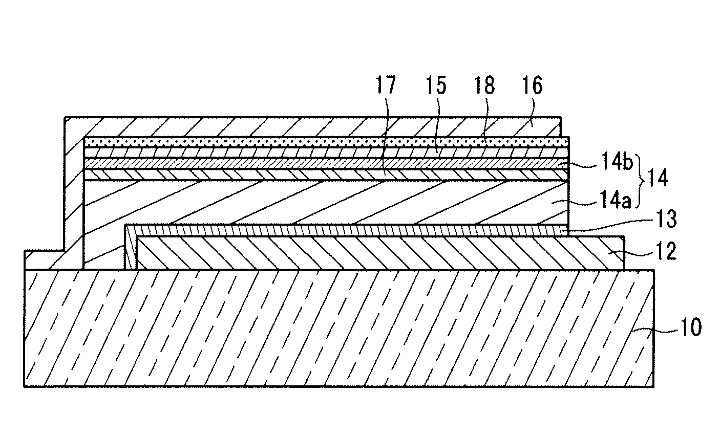
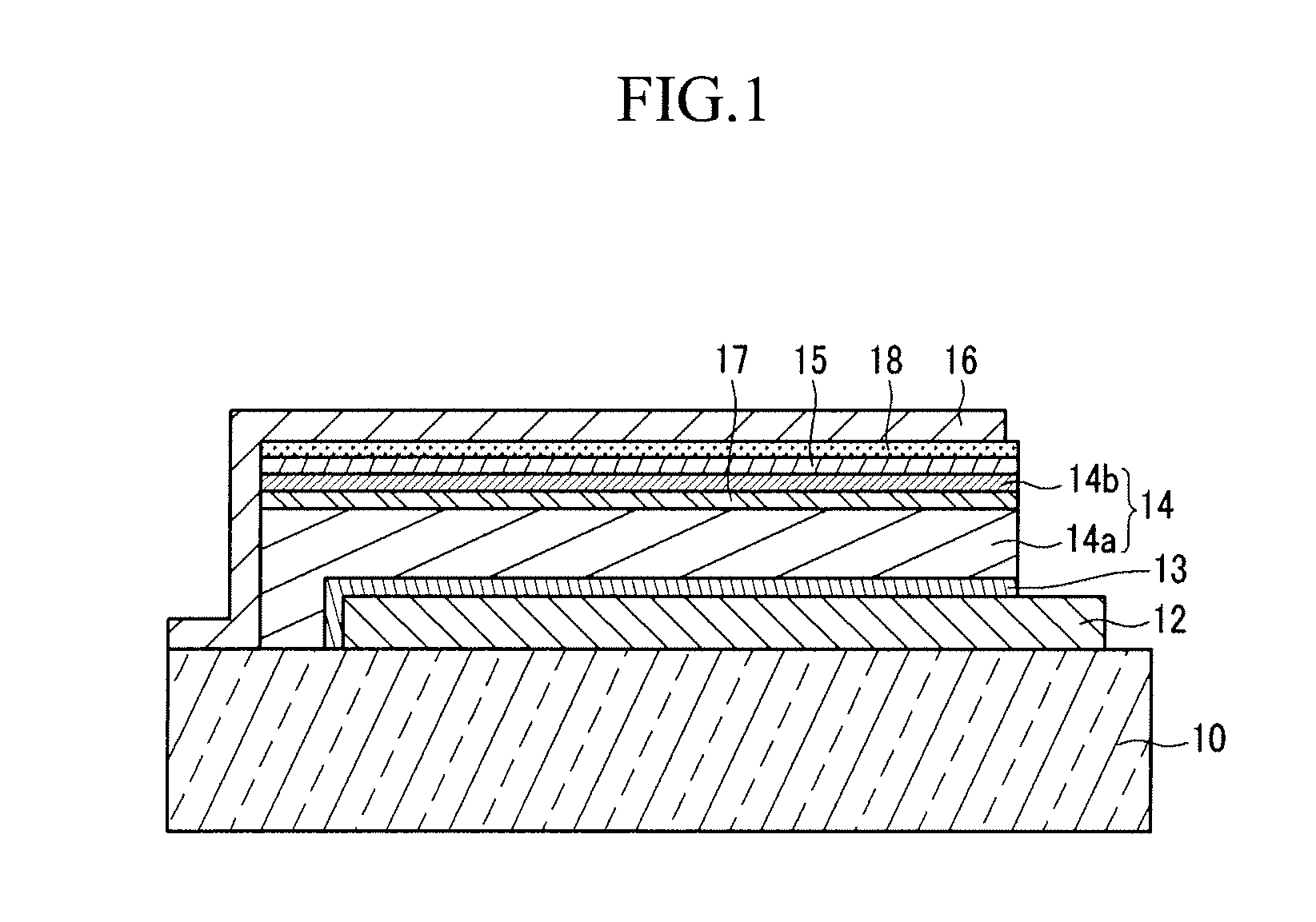
[0032]As such, a photovoltaic device according to an embodiment of the present invention includes a plurality of photovoltaic layers having different light absorption regions, and thereby having relatively high photoelectric efficiency.
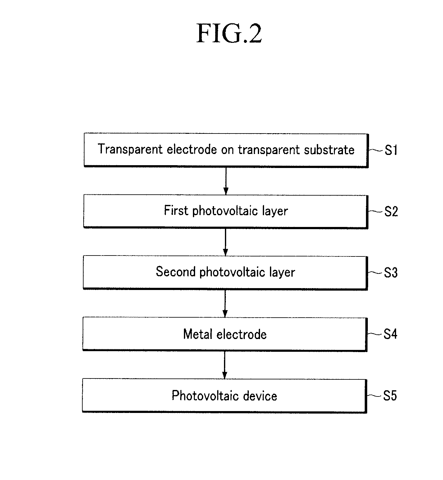
[0033]Also, a manufacturing method according to an embodiment of the present invention allows for disposing a plurality of photovoltaic layers in a photovoltaic device, for uniformly surface-modifying a photovoltaic layer during the plasma surface treatment and thereby generating no pin holes and no dark current, and / or for preventing (or reducing) deterioration of electron conductivity of the surface-treated photovoltaic layer.

Problems solved by technology

However, due to limits in improving photovoltaic device efficiency, photovoltaic devices have been difficult to commercialize.
However, since the photovoltaic device including the inorganic semiconductor is typically fabricated by a plasma CVD method or a high temperature crystal growth process, it requires a lot of energy during the process.
In addition, since the photovoltaic device including the inorganic semiconductor may include environmentally harmful materials such as Cd, As, Se, and the like, it may harm the environment when it is discarded.
Currently, the pn-conjunction type cell does not have sufficient photoelectric efficiency and requires a film deposition process.

Method used


Image

  • Photovoltaic device and method of manufacturing the same
  • Photovoltaic device and method of manufacturing the same
  • Photovoltaic device and method of manufacturing the same

Examples


example 1

[0097]A transparent electrode made of indium tin oxide was disposed on a glass substrate. Then, a composition for a buffer layer was prepared by dissolving a mixture of polyethylene dioxythiophene (PEDOT) and poly(styrenesulfonate) (PSS) (1:1 weight ratio). The composition was then disposed on the transparent electrode by a spin coating method. The coating layer was dried at 100° C. in a vacuum oven for 30 minutes to form a buffer layer with a thickness of about 100 nm.

[0098]Next, a composition for forming a first photovoltaic layer was prepared by dissolving 20 mg of a pentacene derivative as a short-wavelength absorption compound (the pentacene derivation being bis(triisopropylsilylethynyl) pentacene (TIPS-pentacene)) and 20 mg of a fullerene derivative (PCBM) in 1 ml of toluene. Then, the composition was coated on the buffer layer by a spin coating method and dried to form a 100 nm-thick first photovoltaic layer. Then, the first photovoltaic layer was applied with plasma at a sou...

example 2

[0102]A transparent electrode made of indium tin oxide was disposed on a glass substrate. Then, a composition for forming a first buffer layer was prepared by dissolving a mixture of polyethylene dioxythiophene (PEDOT) and poly(styrenesulfonate) (PSS) (1:1 weight ratio) in deionized water on the transparent electrode. The composition was then disposed on the transparent electrode by a spin coating method and dried at 100° C. in a vacuum oven for 30 minutes to form a first buffer layer with a thickness of about 100 nm.

[0103]Then, a composition for forming a first photovoltaic layer was prepared by dissolving 20 mg of a pentacene derivative (bis(triisopropylsilylethynyl) pentacene (TIPS-pentacene)) as a short-wavelength absorption compound and 16 mg of fullerene in 2 ml of chlorobenzene. The composition was coated on the buffer layer by a spin coating method and dried to prepare a 120 nm-thick first photovoltaic layer.

[0104]Then, a composition for forming a second photovoltaic layer w...

example 3

[0108]A transparent electrode including indium tin oxide was disposed on a glass substrate. Then, a composition for forming a buffer layer was prepared by dissolving a mixture of polyethylene dioxythiophene (PEDOT) and poly(styrenesulfonate) (PSS) (1:1 weight ratio) in deionized water. The composition was coated by a spin coating method and dried at 100° C. in a vacuum oven for 30 minutes to dispose a buffer layer with a thickness of about 100 nm.

[0109]Next, a composition for forming a first photovoltaic layer was prepared by dissolving 20 mg of poly(2-methoxy-5-(3,7-dimethoxyoctyloxy)-1,4-phenylene-vinylene) (MDMO-PPV) as a short-wavelength absorption compound and 20 mg of PCBM in 1 ml of toluene. The composition was coated on the buffer layer by a spin coating method to dispose a 100 nm-thick first photovoltaic layer. The first photovoltaic layer was applied with plasma at a source output of 1 W under a nitrogen atmosphere for 30 seconds to perform a surface modifying treatment.

[0...


PUM

PropertyMeasurementUnit
thicknessaaaaaaaaaa
wavelengthaaaaaaaaaa
thicknessaaaaaaaaaa

Abstract

A photovoltaic device having a relatively high photoelectric efficiency and a method of manufacturing the same. The photovoltaic device according to an embodiment of the present invention includes a transparent electrode, a metal electrode, and a plurality of photovoltaic layers between the transparent electrode and the metal electrode. The photovoltaic layers include light-absorbing compounds for absorbing different light absorption wavelength bands, and each of the photovoltaic layers comprises an electron accepting material. As such, a photovoltaic device according to an embodiment of the present invention includes a plurality of photovoltaic layers having different light absorption regions, and thereby having relatively high photoelectric efficiency.

Description

CROSS-REFERENCE TO RELATED APPLICATION[0001]This application claims priority to and the benefit of Korean Patent Application No. 10-2007-0094177, filed in the Korean Intellectual Property Office on Sep. 17, 2007, the entire content of which is incorporated herein by reference.BACKGROUND OF THE INVENTION[0002]1. Field of the Invention[0003]The present invention relates to a photovoltaic device and a method of manufacturing the same.[0004]2. Description of the Related Art[0005]Photovoltaic devices can transform light signals into electrical signals and can be applied to diverse fields such as sensors, solar cells, and the like. Photovoltaic devices are not only environmentally friendly but also have many other advantages such as being a sustainable energy source, having a long life-span, and the like. As such, photovoltaic devices are being actively researched. However, due to limits in improving photovoltaic device efficiency, photovoltaic devices have been difficult to commercialize...

Claims


Application Information

Patent Timeline
Patent Type & Authority Applications(United States)
IPC IPC(8): H01L31/0232H01L31/04H01L31/18
CPCB82Y10/00H01L27/302H01L51/0036H01L51/0037H01L2251/308H01L51/0043H01L51/0046H01L51/4253H01L51/0038Y02E10/50H10K30/57H10K85/113H10K85/1135H10K85/114H10K85/151H10K85/211H10K2102/103H10K30/50H01L31/047H01L31/18H10K30/30
Inventor LEE, MOON-JAEJUNG, BYUNG-JUN
Owner SAMSUNG SDI CO LTD
Learn More