Spin transistor and magnetic memory
a technology which is applied in the field of spin transistor and magnetic memory, can solve the problem of not being able to secure the high id(p)/id(ap) ratio required for applications
- Summary
- Abstract
- Description
- Claims
- Application Information
AI Technical Summary
Problems solved by technology
Method used
Image
Examples
first embodiment
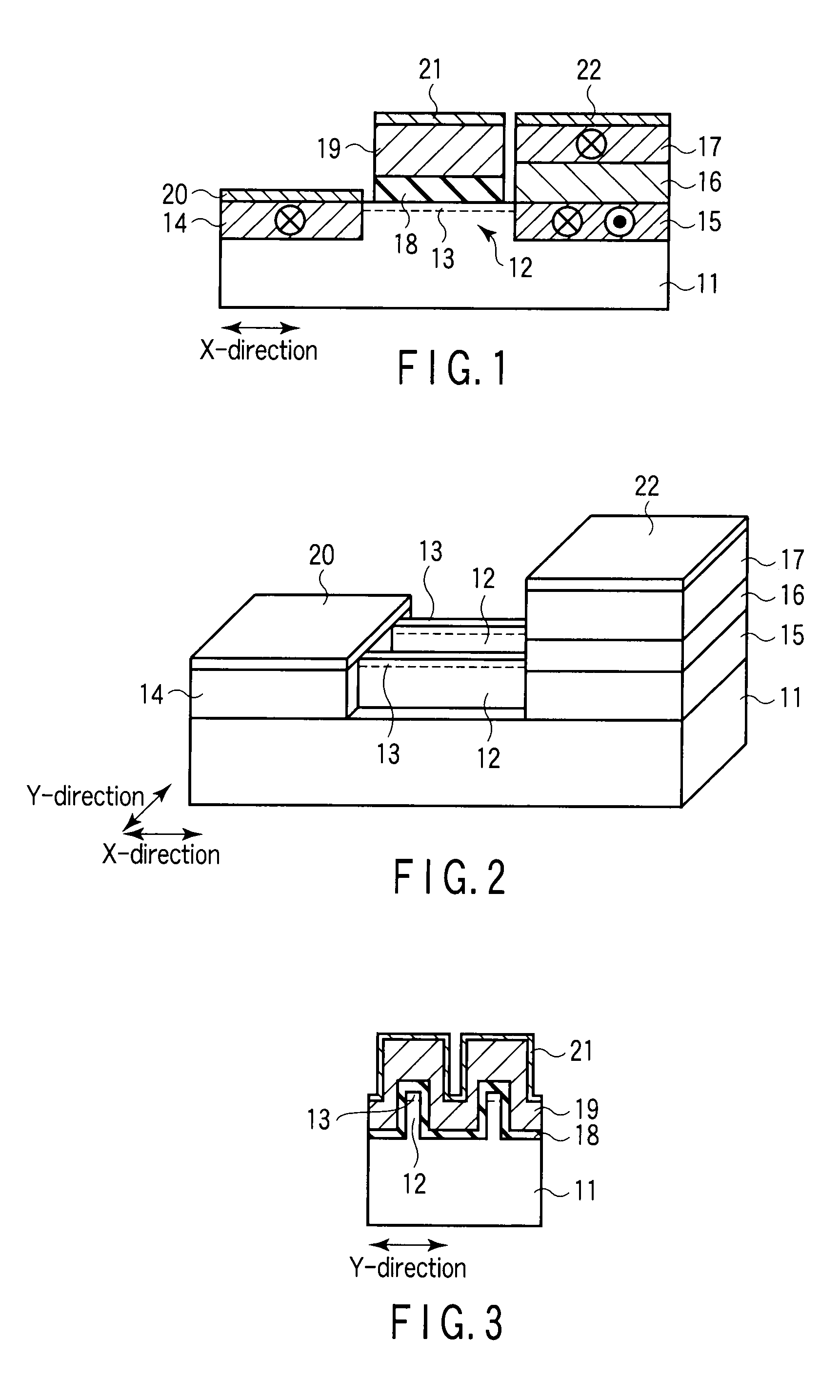
[0045]FIG. 1 is a sectional view illustrating the structure of a spin transistor 10 according to the first embodiment. FIG. 2 is a perspective view illustrating the structure of the spin transistor 10 shown in FIG. 1. FIG. 3 is a sectional view of the spin transistor 10 in which a projecting semiconductor layer (fin) 12 is cut in the Y-direction. Note that a gate electrode 19, gate insulating film 18, and electrode 21 are not shown in FIG. 2 in order to facilitate understanding the structures of the fin 12 and a channel region 13. Note also that FIG. 1 is a sectional view in which the fin 12 shown in FIG. 2 is cut in the X-direction.
[0046]One or more projecting semiconductor layers (fins) 12 extending in the X-direction and having a projecting sectional shape in the Y-direction are formed on a semiconductor substrate 11. Each fin 12 is used as an active layer of the transistor. The number of the fins 12 is not particularly limited. This embodiment exemplarily shows two fins 12.
[0047...
second embodiment
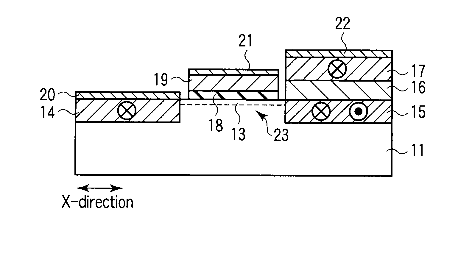
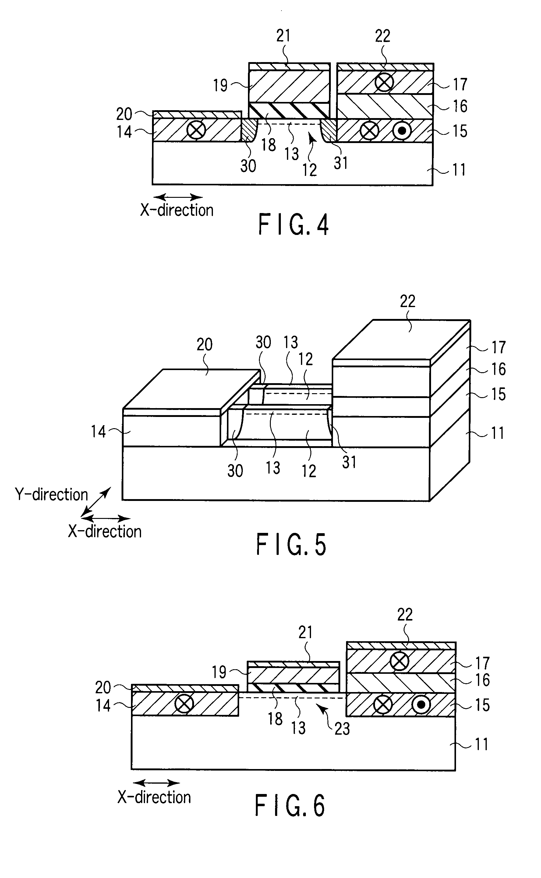
[0094]The second embodiment decreases the width of each channel region 13 by using an inclined step substrate having semiconductor layers 23 having inclined upper surfaces, and forming the channel region 13 in each semiconductor layer 23. Since electrons flow through the narrow channel region 13, spin relaxation is suppressed.
[0095]FIG. 6 is a sectional view illustrating the structure of a spin transistor 10 according to the second embodiment. FIG. 7 is a perspective view illustrating the structure of the spin transistor 10 shown in FIG. 6. FIG. 8 is a sectional view of the spin transistor 10 in which the semiconductor layer 23 is cut in the Y-direction. Note that a gate electrode 19 and gate insulating film 18 are not shown in FIG. 7 in order to facilitate understanding the structure of the semiconductor layer 23 and channel region 13. Note also that FIG. 6 is a sectional view in which the semiconductor layer 23 shown in FIG. 7 is cut in the X-direction.
[0096]An inclined step subst...
third embodiment
[0103]The third embodiment decreases the width of each channel region 13 by forming a plurality of channel regions 13 in a semiconductor substrate 11. Since electrons flow through the narrow channel region 13, spin relaxation is suppressed.
[0104]FIG. 9 is a sectional view illustrating the structure of the spin transistor 10 according to the third embodiment. FIG. 10 is a plan view illustrating the structure of the spin transistor 10 shown in FIG. 9. FIG. 11 is a sectional view of the spin transistor 10 in which the channel region 13 is cut in the Y-direction. Note that a gate electrode 19 and gate insulating film 18 are not shown in FIG. 10 in order to facilitate understanding the structure of the channel region 13. Note also that FIG. 9 is a sectional view in which the channel region 13 shown in FIG. 10 is cut in the X-direction.
[0105]A semiconductor substrate 11 has two openings spaced apart from each other. A first ferromagnetic layer 14 is formed in one opening. A second ferroma...
PUM
 Abstract
Description
Claims
Application Information
 - R&D
- Intellectual Property
- Life Sciences
- Materials
- Tech Scout
- Unparalleled Data Quality
- Higher Quality Content
- 60% Fewer Hallucinations
Browse by: Latest US Patents, China's latest patents, Technical Efficacy Thesaurus, Application Domain, Technology Topic, Popular Technical Reports.
© 2025 PatSnap. All rights reserved.Legal|Privacy policy|Modern Slavery Act Transparency Statement|Sitemap|About US| Contact US: help@patsnap.com


