
Memory access system

Active Publication Date: 2009-02-12
MEGACHIPS
View PDF4 Cites 19 Cited by
  • Summary
  • Abstract
  • Description
  • Claims
  • Application Information

AI Technical Summary

Benefits of technology

[0016]According to this invention, the memory access system corrects errors due to the “program disturb phenomenon” and the “read disturb phenomenon”, in the data in which errors due only to the “read disturb phenomenon” have been detected. The memory access system can avoid or reduce the “read disturb phenomenon” without spending much time for error detection or correction.
[0018]According to this invention, the memory access system detects and corrects errors in read data and scan data. The memory access system corrects errors due to the “program disturb phenomenon” and the “read disturb phenomenon”, in data in which errors due only to the “read disturb phenomenon” have been detected before the errors due to the “read disturb phenomenon” are excessively accumulated. The memory access system can avoid or reduce the “read disturb phenomenon” without increasing the circuit size or spending much time for error detection or correction.
[0019]Therefore, it is an object of the present invention to provide techniques for avoiding unintended rewriting of data or reducing the possibility thereof, due to repeated readouts of data from a non-volatile memory.

Problems solved by technology

Since specific programs are repeatedly read out in the game machines or the like in most cases, however, it begins to be noticed that the programs could be unintendedly rewritten.
But, if there occurs no write operation and only consecutive read operations, it is impossible to recover the function of the unselected cell 53.
This disclosed method, however, can be applied to a memory having a specific cell configuration but can not be applied to any other cell configuration.
In other words, by this method, it is impossible to avoid the “read disturb phenomenon” without depending on cell configurations of memories.

Method used


Image

  • Memory access system
  • Memory access system
  • Memory access system

Examples


first embodiment

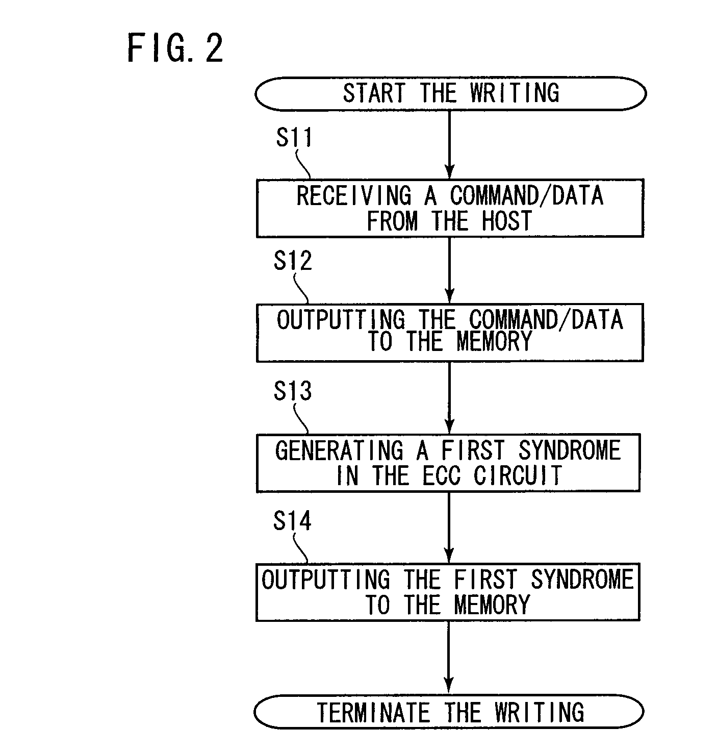
[0033]A first embodiment is described as follows with reference to the drawings. First, the components of a memory access system and of a memory are described. Then, the process flows of the memory access system are described in the following order: (1) a writing process flow, (2) a verification reading process flow after the writing, (3) a normal reading process flow, and (4) a refreshing process flow after error detection.

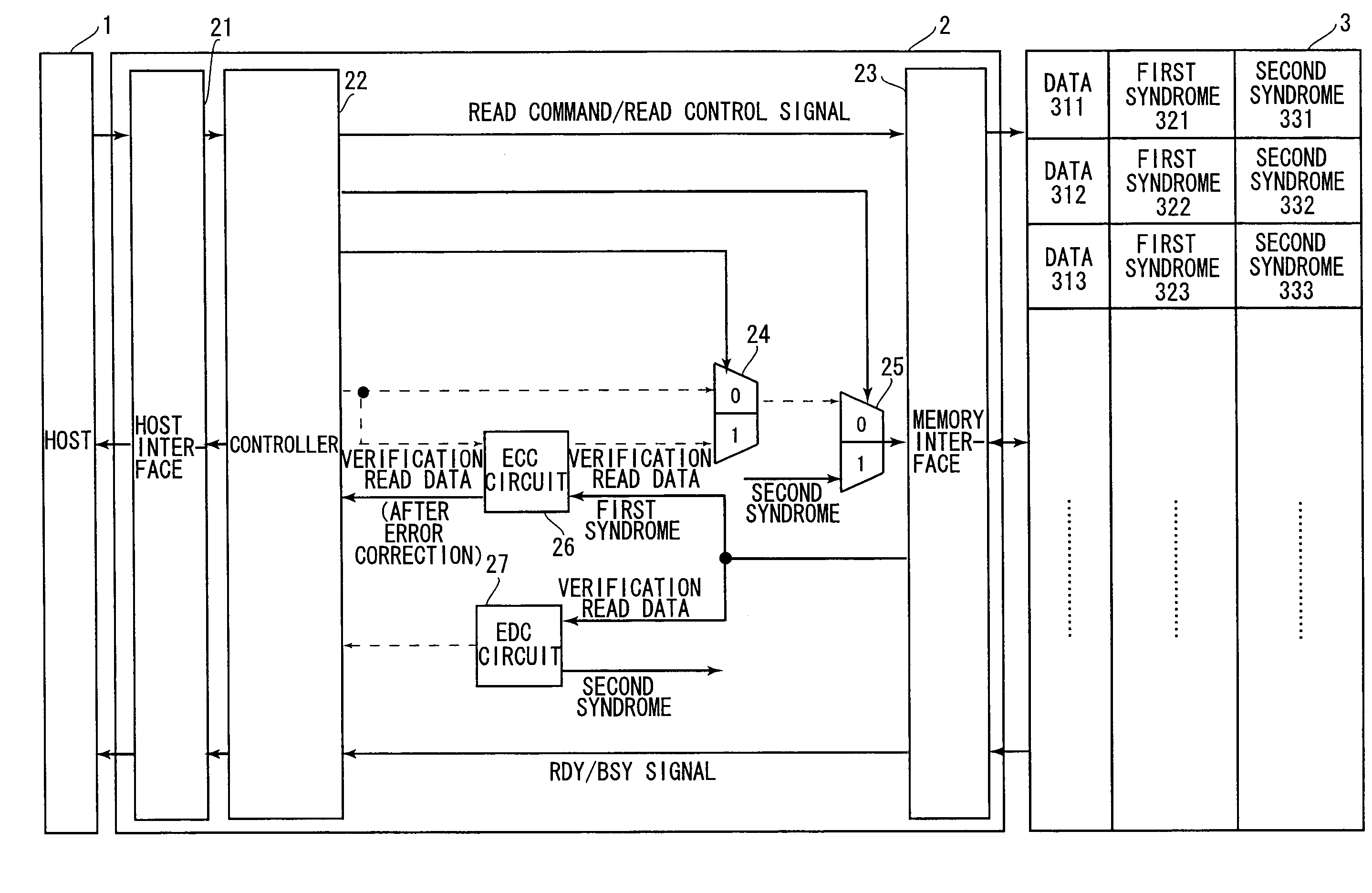
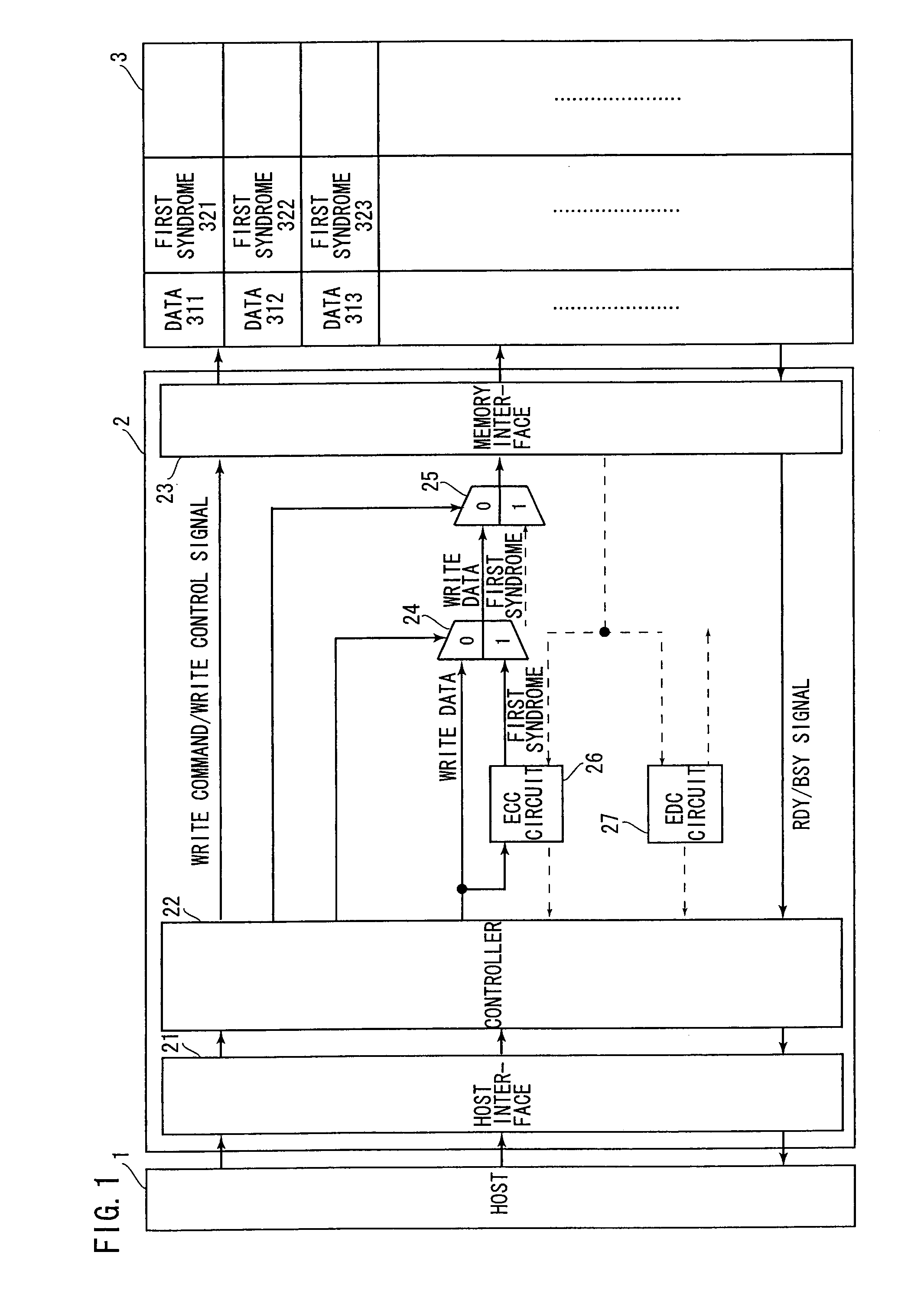
[0034]FIGS. 1, 3, and 5 are block diagrams showing the components of the memory access system and of the memory. FIGS. 1, 3, and 5 also show information exchange in the writing process flow, the verification reading process flow, and the normal reading process flow, respectively.

[0035]The memory access system, which is a system to access a memory 3, is constituted of a host 1 and a memory controller 2 and the like. The host 1 requires the memory controller 2 to write or read data to or from the memory 3. The host 1 also requires the memory controller 2 to inform ...

second embodiment

[0091]A second embodiment is described as follows using FIG. 10. FIG. 10 is a diagram showing an error detection process flow and an error correction process flow according to the second embodiment. The memory controller 2 of the second embodiment differs from that of the first embodiment in having an ECC circuit 28 instead of the ECC circuit 26 and an ECC circuit 29 instead of the EDC circuit 27.

[0092]In the second embodiment, as in the first embodiment, the frequency at which the “program disturb phenomenon” occurs is guaranteed at 4 bits per 512 bytes. The ECC circuit 29 can correct errors of 1 bit per 512 bytes, thereby detecting errors of at least 2 bits per 512 bytes. The ECC circuit 28 can correct errors of 4 bits per 512 bytes.

[0093]The process flows of the second embodiment differ from those of the first embodiment in the error correction process flow (corresponding to Steps S24, S33, and S44). First, the syndrome generation process proceeds as follows. The ECC circuit 28 g...

third embodiment

[0098]A third embodiment is described as follows using FIG. 11. FIG. 11 is a diagram showing an error detection process flow and an error correction process flow according to the third embodiment. The memory controller 2 of the third embodiment differs from that of the first embodiment in having an ECC circuit 30 instead of the ECC circuit 26 and the EDC circuit 27.

[0099]More specifically, in the first embodiment, the ECC circuit 26 and the EDC circuit 27 are composed of different circuit blocks from each other. In the second embodiment, the ECC circuits 28 and 29 are composed of different circuit blocks from each other. In the third embodiment, on the other hand, the ECC circuit 30 is composed of a single circuit block.

[0100]In the third embodiment, in the same manner as in the first embodiment, the frequency at which the “program disturb phenomenon” occurs is guaranteed at 4 bits per 512 bytes. The ECC circuit 30 can correct errors of 5 bits per 512 bytes.

[0101]The process flows o...


PUM


Abstract

The ECC circuit generates the first syndrome of write data, which have not been written to the memory. The EDC circuit generates the second syndrome of verification read data, which have been written to the memory. The EDC circuit detects errors due only to the “read disturb phenomenon” using the second syndrome, the errors occurring in data scanned from the memory. The ECC circuit detects and corrects errors due to the “program disturb phenomenon” and the “read disturb phenomenon” using the first syndrome, the errors occurring in the data in which the errors due only to the “read disturb phenomenon” have been detected. As a result, both the circuit size and the processing time can be reduced.

Description

BACKGROUND OF THE INVENTION[0001]1. Field of the Invention[0002]The present invention relates to a technique to avoid unintended rewriting of data or reduce the possibility thereof, due to repeated readouts of data from a nonvolatile memory.[0003]2. Description of the Background Art[0004]NAND flash memories, among nonvolatile memories, are heavily used for SD memory cards or the like for the purpose of achieving high integration, reduction in manufacturing cost and easy writing for users by simplifying circuit configurations.[0005]In recent, NAND flash memories are adopted for game machines or the like. When the NAND flash memories are used for game machines, there occurs no write operation but only consecutive read operations. In other words, NAND flash memories have been increasingly adopted as ROMs.[0006]Since specific programs are repeatedly read out in the game machines or the like in most cases, however, it begins to be noticed that the programs could be unintendedly rewritten...

Claims


Application Information

Patent Timeline
IPC IPC(8): G11C29/04G06F11/07
CPCG06F11/1068G11C2029/0411G11C2029/0409G11C29/42
Inventor SUGAHARA, TAKAHIKO
Owner MEGACHIPS
Learn More