
Information input device and information input/output device

a technology of information input and information input, which is applied in the direction of instruments, computing, electric digital data processing, etc., can solve the problems of increasing the probability of detection errors, increasing the cost, and deteriorating optical characteristics of products, and achieves high yield and high sensitivity

Inactive Publication Date: 2010-08-05
JAPAN DISPLAY WEST
View PDF9 Cites 37 Cited by
  • Summary
  • Abstract
  • Description
  • Claims
  • Application Information

AI Technical Summary

Benefits of technology

[0027]In view of the above, it is desirable to provide an information input device and an information input / output device which are highly sensitive with good yield.
[0029]In the information input device according to the embodiment of the invention, the position at which the substrate bends can be detected by three or more sensor electrodes, therefore, a touched position in the substrate can be detected, and further, error detection can be reduced by using three or more sensor electrodes.
[0031]In the information input / output device according to the embodiment, the position at which the substrate bends can be detected by three or more sensor electrodes, therefore, a touched position in the substrate can be detected, and further, error detection can be reduced by using three or more sensor electrodes.
[0033]According to the embodiments of the invention, it is possible to obtain an information input device and an information input / output device having high sensitivity as well as high yield.

Problems solved by technology

On the other hand, since the touch panel is arranged at an upper part of the liquid crystal display device, optical characteristics are deteriorated in the products including the touch panel due to effects the thickness, increase of the size or a refractive interface.
There is also a problem of cost increase because the touch panel is necessary in addition to the liquid crystal display device, therefore, integral forming of the liquid crystal display and the touch panel is considered.
However, on another front, when the difference of height between the spacer layer 114 and the sensor electrode 116 is too small, the sensor electrode 116 and the pixel electrode 106 are constantly touched in the case that there exists a conductive foreign matter, which may increase the probability of detection error.
That is to say, there may occur significant problems in yield or quality.
Therefore, the above problems tend to occur.
The above problem of the detection error in the sensor function due to foreign matters may occur not only in the case that the sensor function is included in the liquid crystal display device but also in a configuration in which the sensor function is included in other display devices or a configuration including only the touch panel.

Method used


Image

  • Information input device and information input/output device
  • Information input device and information input/output device
  • Information input device and information input/output device

Examples


first embodiment

1. First Embodiment

Configuration of an Information Input / Output Device

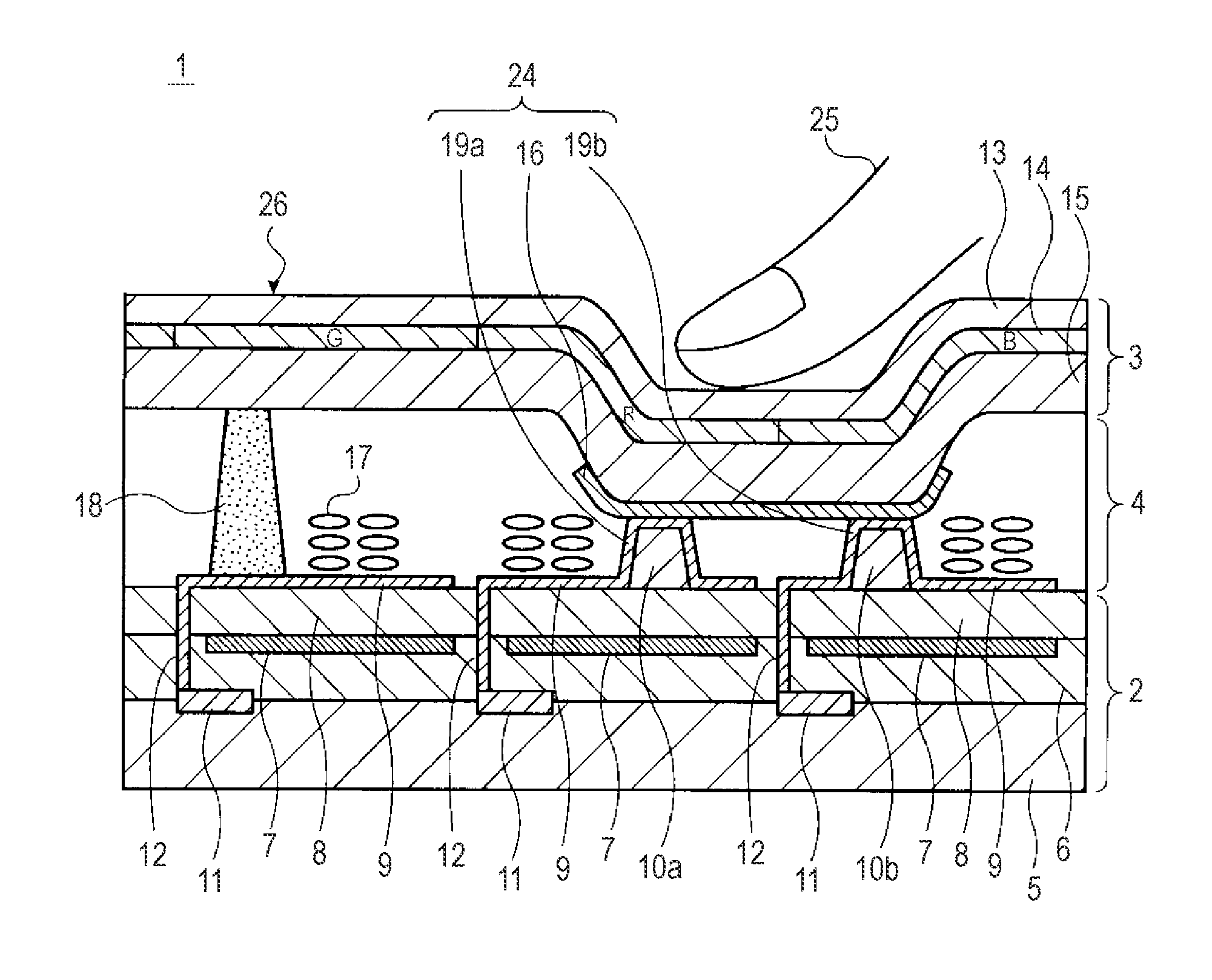
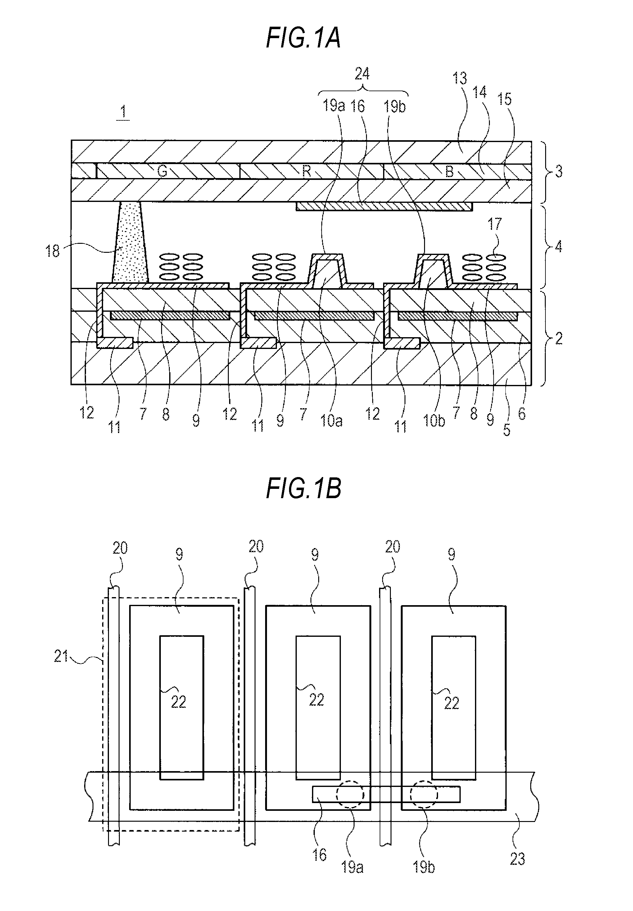
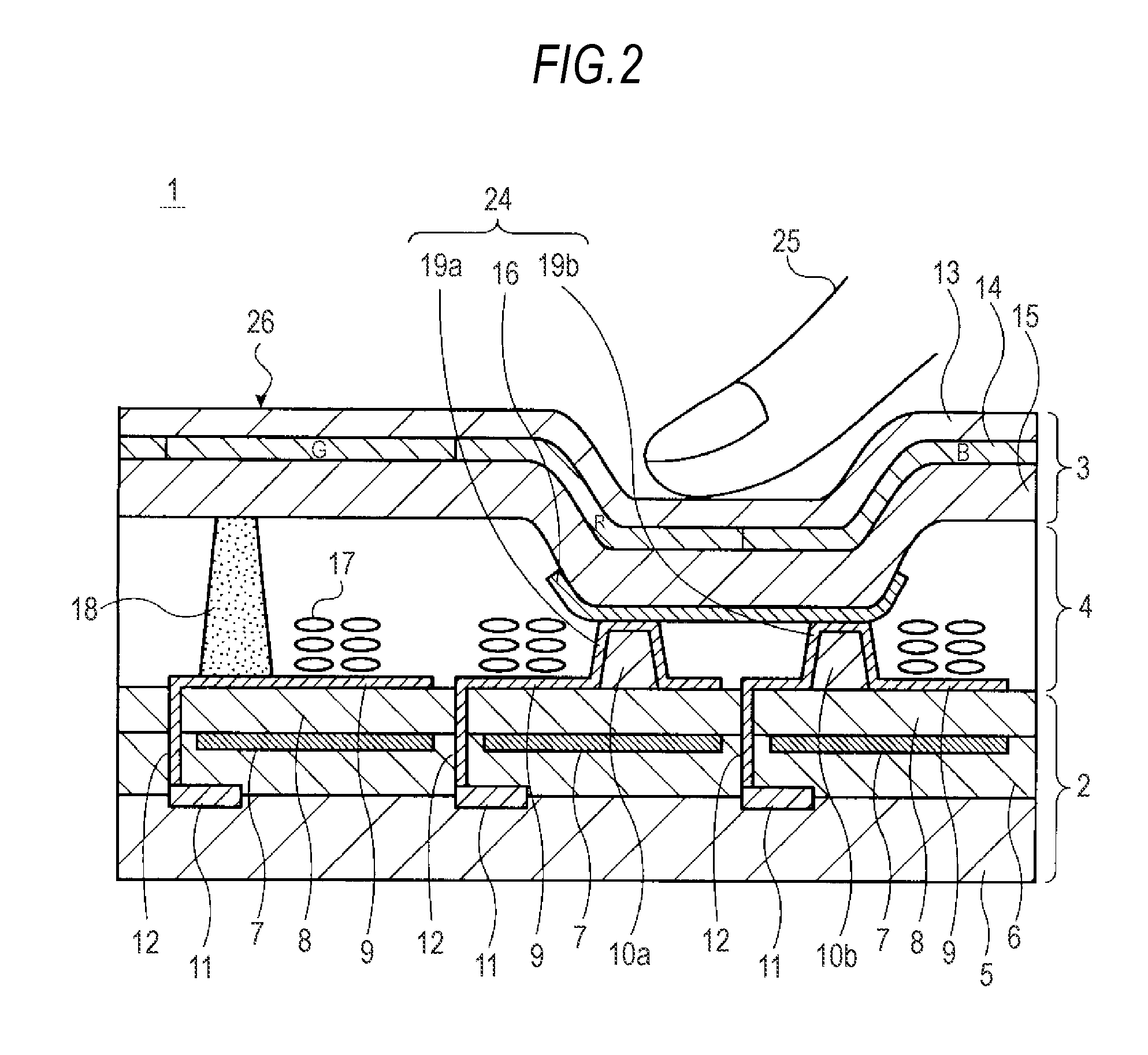
[0058]FIG. 1A and FIG. 1B show a schematic cross-sectional configuration and a planer configuration of an information input / output device according to a first embodiment of the invention. The information input / output device 1 shown in FIG. 1A and FIG. 1B is an example of a liquid crystal display device having a sensor function, that is, an example of a liquid crystal display device including a touch panel.

[0059]As shown in FIG. 1A, the information input / output device 1 according to the embodiment includes a first substrate 2 in which plural thin-film transistors (hereinafter, referred to as TFTs) 11 are formed, a second substrate 3 provided opposite to the first substrate 2 and a liquid crystal layer 4 provided between the two substrates. A position detection portion 24 formed between the first substrate 2 and the second substrate 3 is further included. The first substrate 2, the second substrate 3, the liquid cry...

second embodiment

2. Second Embodiment

Configuration of the Information Input / Output Device

[0109]FIG. 7A and FIG. 7B show a schematic cross-sectional configuration and a plane configuration of an information input / output device according to a second embodiment of the invention. The information input / output device shown in FIG. 7A and FIG. 7B is an example of a liquid crystal display device having a sensor function, namely, an example of a liquid crystal display device including a touch panel. In FIG. 7A and FIG. 7B, the same symbols are given to portions corresponding to FIG. 1A and FIG. 1B and repeated explanation will be omitted.

[0110]The information input / output device according to the embodiment is an example in which the configurations of the pixel electrodes and the position detection portion in the information input / output device 1 according to the first embodiment are partly changed.

[0111]As shown in FIG. 7A and FIG. 7B, in an information input / output device 30 according to the embodiment, two...

modification example 1

of the Second Embodiment

[0119]FIG. 9A shows a schematic plane configuration of a modification example 1 according to the second embodiment and FIG. 9B shows a cross-sectional configuration taken along the line A-A′ of FIG. 9A. In FIG. 9A and FIG. 9B, the same symbols are given to portions corresponding to portions of FIG. 1A and FIG. 1B and repeated explanation will be omitted.

[0120]In the modification example 1, two first sensor electrodes 33a, 33b are formed side by side in a direction orthogonal to the scanning wiring 23 within one pixel 21. Therefore, sensor adjustment layers 32a, 32b formed for securing the height of the first sensor electrodes 33a, 33b are also formed side by side in the direction orthogonal to the direction in which the scanning wiring 23 extends within the unit pixel 21 as shown in FIG. 9B. On the sensor adjustment layer 32a, a pixel electrode 33 of a pixel 21 adjacent to the pixel 21 in which the sensor adjustment layer 32a is formed in an extending manner,...


PUM


Abstract

An information input device includes: a first substrate; a second substrate formed opposite to the first substrate; and a position detection portion including at least three or more sensor electrodes and detecting a position at which at least one of the first substrate and the second substrate bends by electrical change among the sensor electrodes.

Description

BACKGROUND OF THE INVENTION[0001]1. Field of the Invention[0002]The present invention relates to an information input device and an information input / output device.[0003]2. Description of the Related Art[0004]A liquid crystal display device has advantages such that it is thin in thickness and light in weight as well as power consumption of which is low. Therefore, the liquid crystal display device is widely used for electronic apparatuses for mobile applications such as a cellular phone and a digital camera. The liquid crystal display device has a liquid crystal panel in which a liquid crystal layer is sealed between a pair of substrates, in which light irradiated from a planer light source such as a backlight provided on the back surface of the liquid crystal panel is modulated by the liquid crystal panel. Then, images are displayed on the front surface of the liquid crystal panel by the modulated light.[0005]In recent years, a liquid crystal display device having a touch panel is ...

Claims


Application Information

Patent Timeline
Patent Type & Authority Applications(United States)
IPC IPC(8): G06F3/044
CPCG06F3/047G06F3/0412
Inventor KOITO, TAKEOHAYASHI, SHUJITANAKA, TSUTOMUMIZUHASHI, HIROSHIYAMAUCHI, YUKO
Owner JAPAN DISPLAY WEST
Learn More