Electronic device, and information apparatus, communications apparatus, av apparatus, and mobile apparatus using the same

a technology of electronic devices and information devices, applied in the field of electronic devices, can solve the problems of increasing the area and power consumption of the transmitter circuit and the receiver circuit, unreliable data being received, and not being able to accurately achieve the impedance match, so as to achieve the effect of reducing the area and power consumption and speed

Active Publication Date: 2009-02-12
PANASONIC CORP
View PDF11 Cites 11 Cited by
  • Summary
  • Abstract
  • Description
  • Claims
  • Application Information

AI Technical Summary

Benefits of technology

[0012]Thus, the present invention reduces the distortion in the signals transferred through the transmission line, thereby enabling a signal transfer at a higher speed.
[0046]As described above, when a signal is propagated through a conductor line of an electronic device of the present invention, the signal can be propagated to the receiving terminal without introducing a distortion to the voltage waveform thereof. Thus, it is possible to realize a signal transfer at a higher speed than that in the prior art, while reducing the area and the power consumption.

Problems solved by technology

With the configurations of Non-Patent Documents 2 to 6, however, extra circuits need to be added to the transmitter circuit and the receiver circuit, thereby increasing the area and power consumption of the transmitter circuit and those of the receiver circuit.
If the reference resistor is provided inside the semiconductor integrated circuit, the terminating resistor value will then vary due to process variations and temperature variations, whereby it will not be possible to accurately achieve the impedance match.
Then, the signal voltage waveform in the vicinity of the receiver circuit has disturbed phase, resulting in unreliable data being received.

Method used


Image

  • Electronic device, and information apparatus, communications apparatus, av apparatus, and mobile apparatus using the same
  • Electronic device, and information apparatus, communications apparatus, av apparatus, and mobile apparatus using the same
  • Electronic device, and information apparatus, communications apparatus, av apparatus, and mobile apparatus using the same

Examples


first embodiment

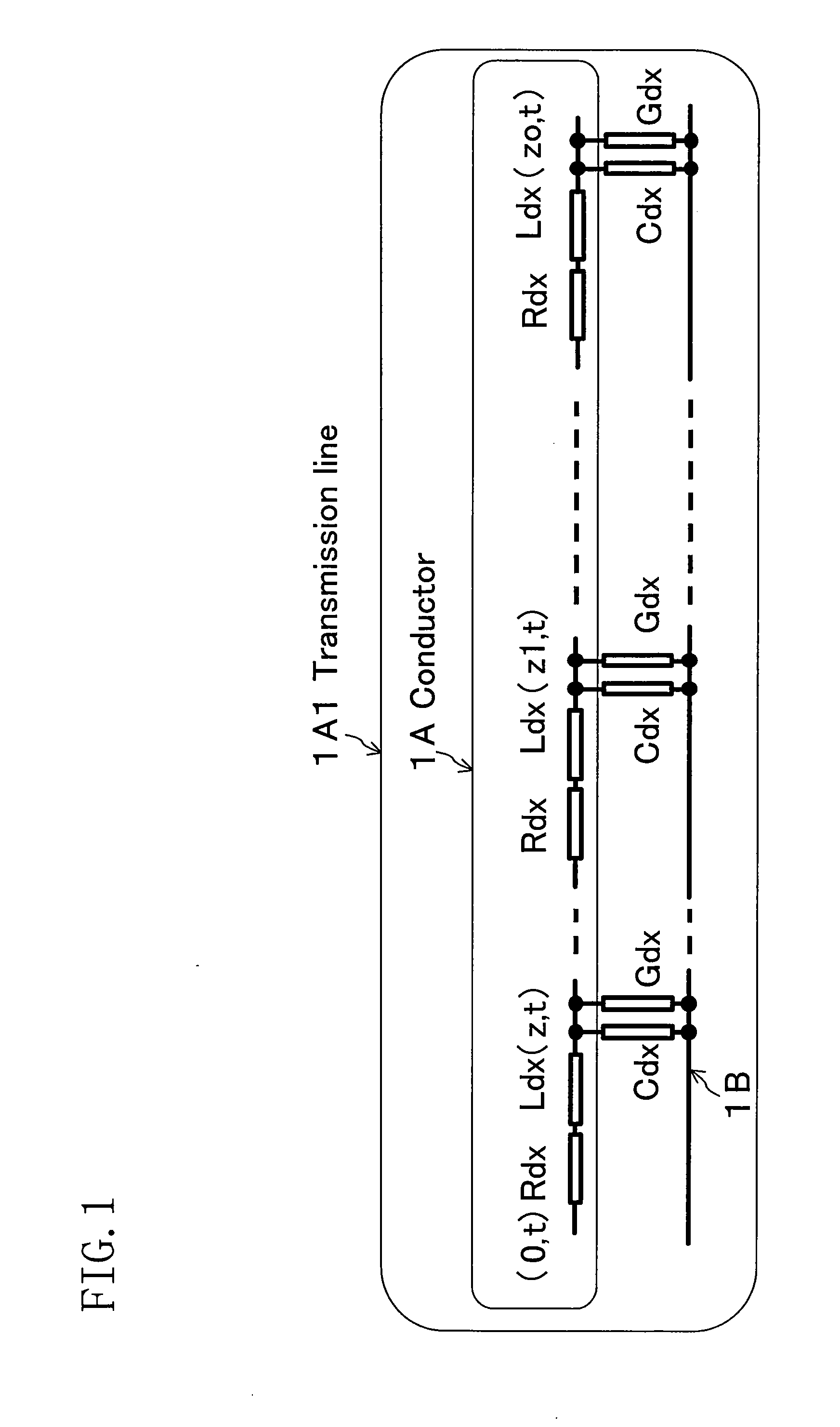
[0091]Referring to FIG. 1, a first embodiment of the present invention is directed to a transmission line 1A1 including a conductor 1A.

[0092]The conductor 1A is herein defined as a substance whose electric resistivity [ohm·m] is on the order of 10−5 or less. The conductor 1A is used as a line for transmitting a signal carrying information. The transmission line 1A1 of the present embodiment is herein defined as a mechanism for propagating an electromagnetic wave therethrough. A transmission line shown without a reference numeral or a reference character refers to a transmission line in general and is not limited to the transmission line 1A1 of the present embodiment. The term “line” is herein used in the same sense as “wire”. The conductor 1A is surrounded by a dielectric substance. The term “being surrounded” as used herein means being substantially surrounded, and the conductor is not necessarily surrounded completely by a dielectric substance. Depending on the process used for ma...

second embodiment

[0171]This embodiment is directed to a correction method, with which the eyepattern of the signal waveform is unlikely to vary due to temperature variations.

[0172]As described above in the first embodiment, the characteristic impedance Z of a line is expressed as shown in Expression 22 for a frequency band in which the resistance of the line is negligible. There is substantially no dependence on the temperature for a frequency band in which the dielectric loss and the skin effect are negligible. For example, for a transmission line using a terminating resistor, the terminating resistor is preferably set to 50 ohm if the characteristic impedance of the line is 50 ohm. In the configuration shown in FIG. 1 of Patent Document 1, if the reference resistor is formed by a copper wire, with the wire being provided in an integrated circuit, the value of the reference resistor varies due to temperature variations of the integrated circuit, and there is an about 2-fold difference over a temper...


PUM


Abstract

An electronic device includes a transmitter circuit, a receiver circuit, a first conductor, and a second conductor of a return path being a grounded line. The first conductor is surrounded by a dielectric. A plurality of resistive elements are connected in parallel between the first conductor and the second conductor. The first conductor transfers therethrough a transmission signal from the transmitter circuit. The length of the line of the first conductor is set to be greater than or equal to one half of the product between the inverse of the signal transfer rate of the first conductor and the velocity of light traveling through the dielectric. The resistive elements are provided along the line of the first conductor for every unit distance being equal to one half of the product between the signal transfer rate of the first conductor and the velocity of light traveling through the dielectric. Thus, it is possible to reduce the signal waveform distortion along the transmission line.

Description

CROSS REFERENCE TO RELATED APPLICATION[0001]This application claims priority under 35 U.S.C. §119 on Patent Application No. 2007-209884 filed in Japan on Aug. 10, 2007 and No. 2008-172484 filed in Japan on Jul. 1, 2008, the entire contents of which are hereby incorporated by reference.BACKGROUND OF THE INVENTION[0002]The present invention relates to an electronic device and, more particularly, to communications within an integrated circuit in an electronic device or between such integrated circuits and to techniques for increasing the operation speed and reducing the area and power consumption by using a transmission line.[0003]A conventional method for high-speed communications within an integrated circuit including a semiconductor in an electronic device or between such integrated circuits includes the use of a transmission line between the transmitter circuit and the receiver circuit. The transmission line includes a device element, with which it is possible to obtain the same im...

Claims


Application Information

Patent Timeline
Patent Type & Authority Applications(United States)
IPC IPC(8): H01P3/00
CPCH01L23/647H01L23/66H01L27/0802H01L2223/6627H01L2924/12044H01L2924/0002H01L2924/1903H01L2924/3011H01L2924/00
Inventor SUMITA, MASAYA
Owner PANASONIC CORP
Why Eureka
Try Eureka