Multilayer ceramic electronic component
a technology of electronic components and ceramics, applied in the direction of fixed capacitor details, fixed capacitors, fixed capacitor terminals, etc., can solve the problems of reducing the reliability of the chip varistor, exhibiting small resistance to abnormal voltages, etc., and achieve the effect of small capacitance and low varistor voltag
- Summary
- Abstract
- Description
- Claims
- Application Information
AI Technical Summary
Benefits of technology
Problems solved by technology
Method used
Image
Examples
exemplary embodiment 1
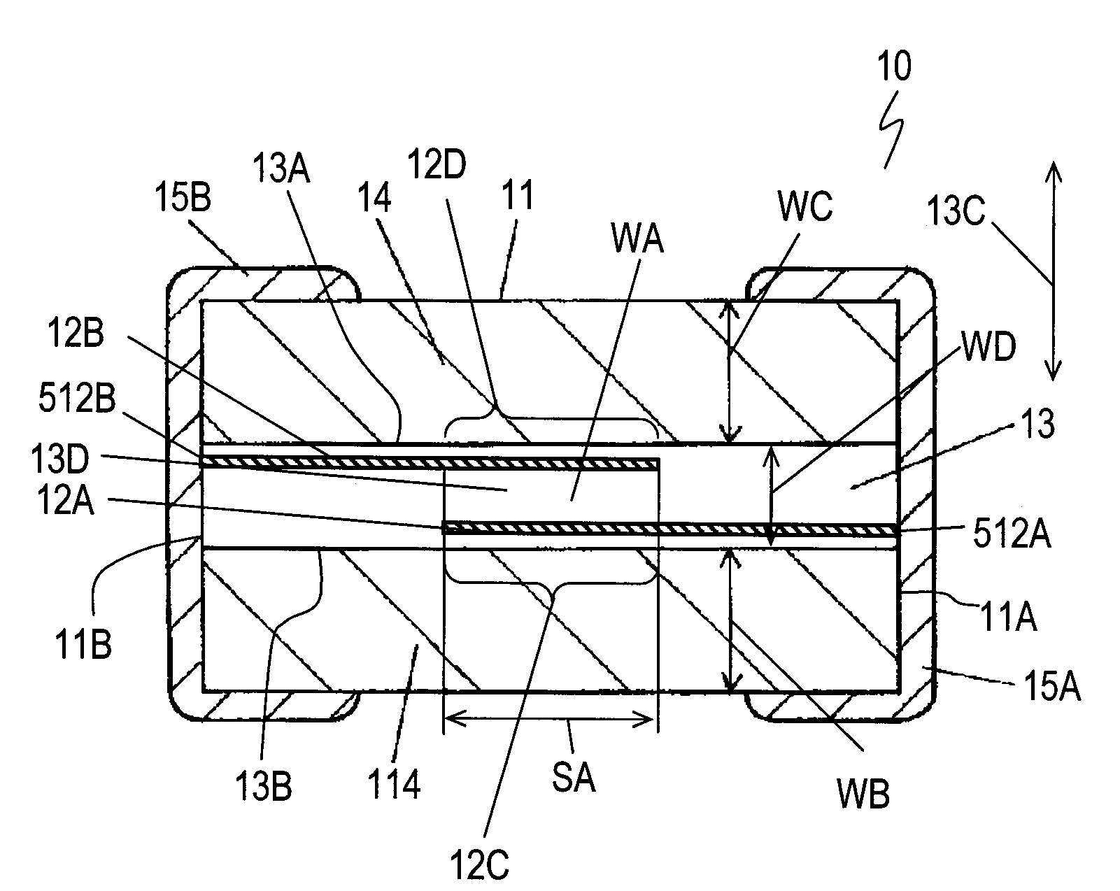
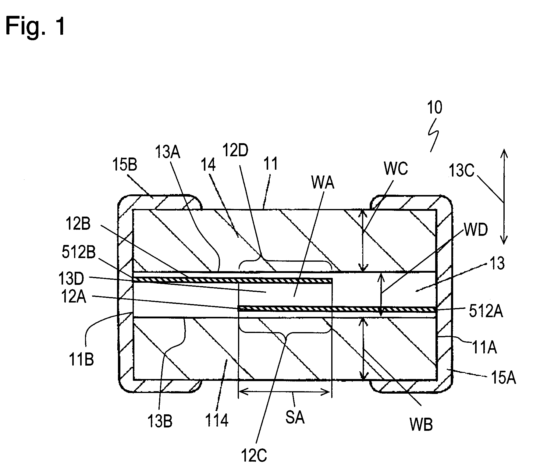
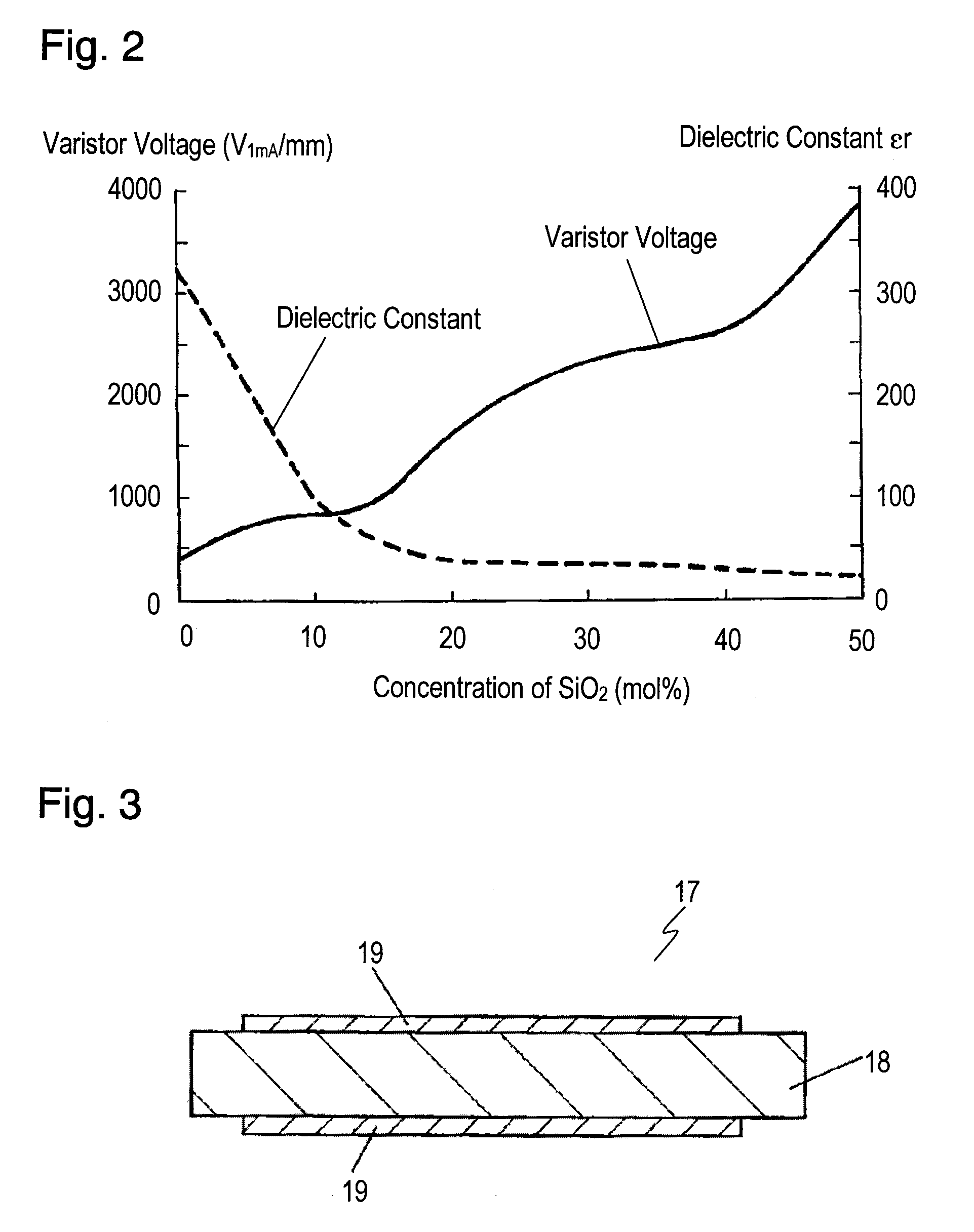
[0029]FIG. 1 shows a sectional view of multilayer chip varistor 10, a multilayer ceramic electronic component, according to Exemplary Embodiment 1 of the present invention. Varistor 10 includes multilayer body 11, internal electrodes 12A and 12B, and external electrodes 15A and 15B. Multilayer body 11 includes ceramic layers 13, 14, and 114. Ceramic layer 13 has surface 13A and surface 13B opposite to surface 13A in direction 13C. Ceramic layer 14 is provided on surface 13A of ceramic layer 13. Ceramic layer 114 is provided on surface 13B of ceramic layer 13. Multilayer body 11 has edge surface 11A and edge surface 11B opposite to edge surface 11A. Internal electrodes 12A and 12B are embedded in ceramic layer 13, are connected to ceramic layer 13, and face each other in direction 13C. Ends 512A and 512B of internal electrodes 12A and 12B expose at edge surfaces 11A and 11B of multilayer body 11, respectively. Ends 512A and 512B of internal electrodes 12A and 12B are connected to ext...
exemplary embodiment 2
[0055]FIG. 4 is a sectional view of multilayer chip varistor 20 in accordance with Exemplary Embodiment 2 of the invention. In varistor 20, components identical to those of multilayer chip varistor 10 shown in FIG. 1 according to Embodiment 1 are denoted by the same reference numerals, and their description will be omitted. Varistor 20 includes multilayer body 21 including ceramic layers 13, 14, and 114 instead of multilayer body 11 of varistor 10. Varister 20 includes internal electrodes 112A and 112B instead of internal electrodes 12A and 12B of varistor 10. Internal electrode 112B is provided on surface 13A of ceramic layer 13 between ceramic layers 13 and 14. Internal electrode 112A is provided on surface 13B of ceramic layer 13 between ceramic layers 13 and 114.
[0056]A method of manufacturing multilayer chip varistor 20 will be described below.
[0057]A predetermined number of the second ceramic green sheets used in varistor 10 so as to provide ceramic layer 14 having a predeterm...
exemplary embodiment 3
[0061]FIG. 5 is a sectional view of multilayer chip varistor 22 in accordance with Exemplary Embodiment 3. In varistor 22, components identical to those of multilayer chip varistor 20 shown in FIG. 4 according to Embodiment 2 are denoted by the same reference numerals, and their description will be omitted. Varistor 22 includes multilayer body 21 including ceramic layers 13, 14, and 114. Multilayer body 21 is covered with film 16 made of Zn—Si—O-based compound containing mainly Zn2SiO4.
[0062]The Zn—Si—O-based compound contains mainly non-stoichiometric compound consisting of Zn, Si, and O (i.e., the ratio of Zn:Si:O is not equal to 2:1:4), and further contains Bi and Sb. For example, this non-stoichiometric compound is ZnxSiyOz, ZnxSiyBimOz, or ZnxSiySbnOz, where, x, y, z, m, and n are natural numbers.
[0063]A method of manufacturing multilayer chip varistor 22 will be described below:
[0064]An unsintered body which is to be multilayer body 21 by a method similarly to that of manufact...
PUM
| Property | Measurement | Unit |
|---|---|---|
| electric current | aaaaa | aaaaa |
| electric current | aaaaa | aaaaa |
| size | aaaaa | aaaaa |
Abstract
Description
Claims
Application Information
 - R&D
- Intellectual Property
- Life Sciences
- Materials
- Tech Scout
- Unparalleled Data Quality
- Higher Quality Content
- 60% Fewer Hallucinations
Browse by: Latest US Patents, China's latest patents, Technical Efficacy Thesaurus, Application Domain, Technology Topic, Popular Technical Reports.
© 2025 PatSnap. All rights reserved.Legal|Privacy policy|Modern Slavery Act Transparency Statement|Sitemap|About US| Contact US: help@patsnap.com


